Download
1 / 18
180 likes | 201 Vues
This document outlines the LHCb readout scheme, data acquisition process, optical links utilization, event building network, and common requirements. It covers trigger rates, buffering, bandwidth needs, data flow on the board, synchronization, and trigger processing levels.

E N D
TELL1A common data acquisition board for LHCb Guido Haefeli, University of Lausanne
Outline • LHCb readout scheme • LHCb data acquisition • Optical links • Event building network • Common readout requirements • Trigger rates • Buffers • Bandwidth • Data flow on the board • Synchronization • Level 1 trigger pre-processing and zero-suppression • Higher level trigger processing • Gigabit Ethernet interface • Board implementation • FPGAs • Level 1 buffer • Higher level trigger multi event packet buffer • Summary
LHCb trigger system L0: fully synchronous and pipelined fixed latency • Pile-Up • Calorimeter • Muon L1: software trigger with maximal latency • VELO • TT • (Outer Tracker) HLT: software trigger • Access to all sub-detectors
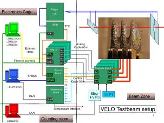
LHCb data acquisition TELL1 in counting room Front End of detectors in cavern 60-100m
TELL1 Switch Switch Switch Switch Switch SFC SFC SFC SFC Switch Switch Switch Switch Commercial network equipment CPU CPU CPU CPU CPU CPU CPU CPU CPU CPU CPU CPU Level-1 Traffic Gb Ethernet HLT Traffic Mixed Traffic Event building network HLTTraffic 40KHz MEP /16 Mux x8 Level-1Traffic 1.11MHz MEP /32 Mux x2 SFC /94 Front-end Electronics TRM FE FE FE FE FE FE FE FE FE FE FE FE Multiplexing Layer Readout Network L1-Decision Sorter 94 Links 7.1 GB/s … 94 SFCs CPUFarm ~1800 CPUs
Trigger rates and buffering • Max. L0 Accept rate = 1.11 MHz • Max. L1 Accept rate = 40 KHz • L0 buffer is implemented on the Front End fixed to be 160 clock cycles ! • L1 buffer 58254 events which equals to 52.4us !
Bandwidth requirements • Input data bandwidth for a 24 optical link motherboard • Optical receiver 24 fibres x 1.28 Gbit/s 30.7Gbit/s • Analog receiver 64 channels x 10-bit @ 40 MHz 25.6 Gbit/s • L1 Buffer • Write data bandwidth 30.7 Gbit/s • Read data bandwidth 4 Gbit/s • DAQ links • 4 Gigabit Ethernet links • ECS • 10/100 Ethernet for remote control
A bit of history • L1 trigger scheme changed • During the last year the maximal L1T latency has increased from 1.8ms to 52ms (x32). This forces the change SRAM FIFO SDRAM • Detectors added to L1T (TT, OT) and potentially others • Decreasing cost for the optical links data processing is done in the counting room • More and more functionalities on the read out board because no Readout Unit and no Network Processors! • The event fragments are packed in so called “Multi Event Packets” MEP to optimize ethernet packet size and packet rate. • The acquisition board adds IP destination, does Ethernet framing and transmit data buffering …)
How can we use a common read out ? FE FE FE FE Adaptation to two link system is possible with receiver mezzanine cards. A-RxCard A-RxCard O-RxCard FPGAs allow the adaptation for different data processing. PP-FPGA PP-FPGA PP-FPGA PP-FPGA L1B L1B L1B L1B SyncLink-FPGA Sufficient bandwidth for the entire acquisition path FEM ECS TTCrx RO-Tx Mezzanine card for detector specific needs ECS L0 and L1 Throttle TTC L1T HLT
Advantages being common ! FE FE FE FE Solution for new system requirements can be found regarding the architecture of one readout board only. A-RxCard A-RxCard O-RxCard PP-FPGA PP-FPGA PP-FPGA PP-FPGA Cost reduction due bigger quantity serial production (300 board for LHCb). L1B L1B L1B L1B SyncLink-FPGA Reduce maintenance cost with a single system. FEM ECS TTCrx RO-Tx ECS L0 and L1 Throttle TTC L1T HLT A lot of common software interfaces.
32 32 64 64 64 16 8 8 8 8 32 32 32 32 32 32 32 32 32 16 FIFO FIFO FIFO L1T dataflow X12 SyncLink-FPGA PP-FPGA O-RxCard PP-FPGA PP-FPGA TTC broadcast PP-FPGA ECS L1T IP RAM L1T DEST FIFO L1T Link FIFO FIFO O-RxCard (Mezzanine card) L1PP X12 L1T Framer RO-Interface POS-Level 3 Data Link L1T MEP Buffer FIFO FIFO FIFO L1PP 64 Kbyte 1 Kbyte Shared data path for 2 channel RO-TxCard @ 100 MHz ID Check Sync FIFO Cluster encapsulation FIFO L1PP 1 Kbyte L1B FIFO L1PP 64 KByte internal SRAM @ 100 MHz Link DDR @80MHz @80MHz
HLT dataflow Sync Sync FIFO FIFO ID Check ID Check FIFO FIFO Sync Sync FIFO FIFO 32 32 32 32 32 32 32 32 32 16 32 32 16 32 16 32 32 32 16 16 16 32 16 16 16 16 FIFO FIFO FIFO 0.9us/event 20us/event 320us/MEP SyncLink Stratix 1S25, 25K LE PP-FPGA, Altera Stratix 1S20, 18K LE X12 FIFO O-RxCard TTC broadcast PP-FPGA FIFO ECS PP-FPGA HLT IP RAM HLT DEST FIFO HLT ZeroSupp Event Encaps. FIFO FIFO HLT Framer RO-Interface POS-Level 3 X12 HLT MEP Buffer O-RxCard (Mezzanine card) Data link FIFO FIFO L1B 4 Kbyte Shared data path for 2 channel RO-TxCard @ 100 MHz 1 Kbyte 1 Kbyte Sync FIFO ID Check FIFO Sync FIFO 1 Mbyte external QDR SRAM @ 100 MHz Link DDR @80MHz @80MHz @120MHz @120MHz 64 KEvent DDR SDRAM
O-RxCard LOW V POWER PP FPGA Glue Card CCPC L1B HLT MEP PP FPGA Sync Link FPGA TTCrx PP FPGA FEM A-RxCard RO-TxCard PP FPGA
Equal length signal traces are required for DDR SDRAM Implementation (4 x 48-bit wide bus @ 240MHz data transfer rate ! (46 Gbit/s) DDR bank data signal layout
Summary • After evaluating different concepts for data processing and acquisition a common read out board for LHCb has been specified and designed. • It serves for 24-optical with a data transfer rate of 1.28 Gbit/s each. • The board implements data identification, L1 buffering an zero suppression. • It is made for the use with standard Gigabit ethernet equipment as switches and routers.