Download
1 / 180
1.9k likes | 2.31k Vues
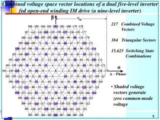
Combined voltage space vector locations of a dual five-level inverter fed open-end winding IM drive (a nine-level inverter). 217 Combined Voltage Vectors Triangular Sectors 15,625 Switching State Combinations. Shaded voltage vectors generate zero common-mode

E N D
Combined voltage space vector locations of a dual five-level inverter fed open-end winding IM drive (a nine-level inverter) • 217 Combined Voltage • Vectors • Triangular Sectors • 15,625 Switching State • Combinations • Shaded voltage • vectors generate • zero common-mode • voltage CEDT, INDIAN INSTITUTE OF SCIENCE, BANGALORE, INDIA
Common-mode voltage of the dual five-level inverter fed open-end winding IM drive • Common-mode voltage generated by individual five-level inverters • (Inverter-A or Inverter-A’) Inverter-A Inverter-A’ • Common-mode voltage in the phase voltage of induction motor with • the proposed dual five-level inverter fed drive CEDT, INDIAN INSTITUTE OF SCIENCE, BANGALORE, INDIA
Groups of common-mode voltage generated by individual five-level inverter CEDT, INDIAN INSTITUTE OF SCIENCE, BANGALORE, INDIA
Voltage vectors and corresponding switching states resulting into zero common-mode voltage in individual five-level inverter (Inv.-A or Inv.-A’) 19 Voltage Vectors 24 Triangular Sectors 19 Switching States • All the shaded switching • states belong to the • Group-7,which generate • zero common-mode • voltage at the inverter • poles
Combined voltage space phasor locations resulting into zero common-mode voltage (a five-level inverter voltage space phasor structure) 61 Combined Voltage Vectors 96 Triangular Sectors 361 Switching State Combinations • Achieved when individual • five-level inverters (Inv.-A • and Inv.-A’) are switched • using the switching states • belonging to the Group-7 • only.
Number of redundant switching states available for each voltage vectors of the five-level inverter with zero common-mode voltage 61 Combined Voltage Vectors 96 Triangular Sectors 361 Switching Stats Combinations • Achieved when individual • five-level inverters (Inv.-A • and Inv.-A’) are switched • using the switching states • belonging to the Group-7 • only.
Some of the voltage vectors and their redundant switching states for five-level inverter with zero common-mode voltage CEDT, INDIAN INSTITUTE OF SCIENCE, BANGALORE, INDIA
Amplitude of maximum reference space vector possible in linear range of modulation without boost in the DC-link of the proposed inverter CEDT, INDIAN INSTITUTE OF SCIENCE, BANGALORE, INDIA
Generation of same maximum peak fundamental amplitude of the phase voltage equivalent to that of a conventional SVPWM based five-level inverter • A boost of 15% in the dc-link of the proposed drive is • required to generate the maximum peak fundamental • amplitude of the phase voltage equivalent to that of a • conventional SVPWM based five-level inverter. CEDT, INDIAN INSTITUTE OF SCIENCE, BANGALORE, INDIA
Voltage space vector locations for proposed five-level inverter with common-mode voltage elimination (with dc-link boost) 61 Combined Voltage Vectors 96 Triangular Sectors 361 Switching Stats Combinations CEDT, INDIAN INSTITUTE OF SCIENCE, BANGALORE, INDIA
Switching state combination selected to generate the voltage space phasors of five-level inverter with zero CMV 61 Combined Voltage Vectors 96 Triangular Sectors 61 Switching Stats Combinations CEDT, INDIAN INSTITUTE OF SCIENCE, BANGALORE, INDIA
Power scheme of the proposed five-level inverter with CME CEDT, INDIAN INSTITUTE OF SCIENCE, BANGALORE, INDIA
Experimental results Pole voltage (VAO) Two-level operation Y-axis: 1 div. = 50 V X-axis: 1 div. = 10 ms Phase voltage (VA’A) Pole voltage (VA’O) Phase voltage FFT (two-level operation) Y-axis: Normalized amplitude X-axis: Order of harmonic Pole voltage FFT (two-level operation) Y-axis: Normalized amplitude X-axis: Order of harmonic CEDT, INDIAN INSTITUTE OF SCIENCE, BANGALORE, INDIA
Experimental results (contd…) Pole voltage (VAO) Three-level operation Y-axis: 1 div. = 40 V X-axis: 1 div. = 10 ms Phase voltage (VA’A) Pole voltage (VA’O) Phase voltage FFT (three-level operation) Y-axis: Normalized amplitude X-axis: Order of harmonic Pole voltage FFT (three-level operation) Y-axis: Normalized amplitude X-axis: Order of harmonic CEDT, INDIAN INSTITUTE OF SCIENCE, BANGALORE, INDIA
Experimental results (contd…) Pole voltage (VAO) Four-level operation Y-axis: 1 div. = 70 V X-axis: 1 div. = 5 ms Phase voltage (VA’A) Pole voltage (VA’O) Phase voltage FFT (four-level operation) Y-axis: Normalized amplitude X-axis: Order of harmonic Pole voltage FFT (four-level operation) Y-axis: Normalized amplitude X-axis: Order of harmonic CEDT, INDIAN INSTITUTE OF SCIENCE, BANGALORE, INDIA
Experimental results (contd…) Pole voltage (VAO) Five-level operation Y-axis: 1 div. = 75 V X-axis: 1 div. = 5 ms Phase voltage (VA’A) Pole voltage (VA’O) Phase voltage FFT (five-level operation) Y-axis: Normalized amplitude X-axis: Order of harmonic Pole voltage FFT (five-level operation) Y-axis: Normalized amplitude X-axis: Order of harmonic CEDT, INDIAN INSTITUTE OF SCIENCE, BANGALORE, INDIA
Experimental results (contd…) Pole voltage (VAO) Over-modulation operation Y-axis: 1 div. = 80 V X-axis: 1 div. = 5 ms Phase voltage (VA’A) Pole voltage (VA’O) Phase voltage FFT (over-modulation operation) Y-axis: Normalized amplitude X-axis: Order of harmonic Pole voltage FFT (over-modulation operation) Y-axis: Normalized amplitude X-axis: Order of harmonic CEDT, INDIAN INSTITUTE OF SCIENCE, BANGALORE, INDIA
Experimental results (contd…) Phase voltage (VA’A) Y-axis: 1 div. = 50 V Four-level operation X-axis: 1 div. = 5 ms Phase current Y-axis: 1 div. = 1 A Phase voltage (VA’A) Y-axis: 1 div. = 50 V Five-level operation X-axis: 1 div. = 5 ms Phase current Y-axis: 1 div. = 1 A CEDT, INDIAN INSTITUTE OF SCIENCE, BANGALORE, INDIA
Salient features of the proposed common-mode elimination scheme for multilevel inverter fed drive • A dual five-level inverter fed open-end winding induction motor • drive with elimination of common-mode voltage in the entire • operating range. • Each five-level inverter of the proposed drive is formed by • cascading two conventional two-level inverters and a conventional • three-level NPC inverter. Hence, the proposed drive offers simple • power-bus structure compared to the five-level NPC inverter fed • drive. • There is no alternating common-mode voltage in the inverter • poles as well as at the phase windings of the induction machine. CEDT, Indian Institute of Science CEDT, INDIAN INSTITUTE OF SCIENCE, BANGALORE, INDIA
Salient features of proposed common-mode elimination scheme for multilevel inverter fed drive (contd…) • A common DC-link is used at both the ends of the open-end • winding induction machine, for both the five-level inverters. • The DC-link voltage requirement of proposed open-end winding • IM drive is nearly half as compared to that of a single five-level • inverter fed conventional IM drive. • Hence, the voltage stress on the devices is reduced and devices • with lower voltage blocking capability can be used, which makes • the proposed drive scheme suitable for high power applications. CEDT, INDIAN INSTITUTE OF SCIENCE, BANGALORE, INDIA
In the implemented scheme, the rotor flux position is estimated from the motor phase current ripples During the low speed region of operation, the current ripple during the zero vector periods are used for rotor flux position estimation During the high speed region of operation, the current ripple during the active vector periods are used for rotor flux position estimation The scheme is implemented for a three phase motor, but the scheme can be extended to any multi phase motor and also with open-end winding structure CONCLUSION CEDT, INDIAN INSTITUTE OF SCIENCE, BANGALORE, INDIA
Linearization of the Multi-level SVPWM in Over-modulation Region By R. S. Kanchan, P. N. Tekwani, and K. Gopakumar Centre for Electronic Design and Technology, Indian Institute of Science Bangalore, INDIA CEDT, INDIAN INSTITUTE OF SCIENCE, BANGALORE, INDIA
v v v AN BN CN 0.5 Reference signals Vt and carrier V /2 dc -0.5 a0 V -V /2 dc V /2 dc b0 V -V /2 dc V /2 dc c0 2 π 3 π/2 (wt) π/2 π V -V /2 dc Linearization of the Multi-level SVPWM in the Over-Modulation Region Conventional two-level Sine-Triangle PWM The fundamental component in the output PWM waveform is equal to k = (peak amplitude of the sinusoidal reference) / (height of the triangular carrier signal) • Three sinusoidal (1200 phase shifted) reference signals are compared with triangular carrier • The PWM signals are generated for three phases • The pole voltage is clamped to +ve DC link bus if Vref >Vt else to –ve DC link bus CEDT, INDIAN INSTITUTE OF SCIENCE, BANGALORE, INDIA
V V V CN AN BN V /2 dc -V /2 dc V /2 dc a0 V -V /2 dc V /2 dc b0 V -V /2 dc V /2 dc c0 V -V /2 dc (wt) 3 π/2 π 2 π π/2 Linearization of the Multi-level SVPWM in the Over-Modulation Region Conventional Sine-Triangle PWM: Over-Modulation Range • When ref signal is greater than carrier, the pole voltages are clamped to the DC link bus voltage • The fundamental component in output PWM waveform is not given by • But there is reduction in the fundamental component in the output voltage CEDT, INDIAN INSTITUTE OF SCIENCE, BANGALORE, INDIA
0.5 0 π/2 π 00 wt Linearization of the Multi-level SVPWM in the Over-Modulation Region Conventional Sine-Triangle PWM: Over-Modulation Range • Reduction in the output fundamental is proportional to the shaded area CEDT, INDIAN INSTITUTE OF SCIENCE, BANGALORE, INDIA
0.637 0.50 Non-linear characteristic k Linear range Over-modulation 0.7854 MI Linearization of the Multi-level SVPWM in the Over-Modulation Region Conventional Sine-Triangle PWM • The voltage transfer characteristics i.e the ratio between the output fundamental and the reference signal amplitude is non-linear in the over-modulation region CEDT, INDIAN INSTITUTE OF SCIENCE, BANGALORE, INDIA
v*BN v*CN v*AN 0.5 and carrier Reference signals -0.5 200 400 600 800 1000 1200 1400 1600 1800 V /2 dc a0 V -V /2 dc 200 400 600 800 1000 1200 1400 1600 1800 V /2 dc b0 V -V /2 dc 200 400 600 800 1000 1200 1400 1600 1800 V /2 1 dc c0 V -V /2 dc 2 π 3 π/2 π/2 π (wt) Linearization of the Multi-level SVPWM in the Over-Modulation Region Carrier based Space-Vector PWM (SVPWM) • The reference signals are added with an offset voffset1 • The resultant PWM is a Space Vector PWM CEDT, INDIAN INSTITUTE OF SCIENCE, BANGALORE, INDIA
0.5 0 π/2 00 wt π/6 π/3 2π/3 π Linearization of the Multi-level SVPWM in the Over-Modulation Region Carrier based Space-Vector PWM (SVPWM) • Again when ref signal is greater than carrier, the pole voltages are clamped to the DC link bus voltage • There is reduction in the fundamental component in the output voltage • Reduction in the output fundamental is proportional to the shaded area CEDT, INDIAN INSTITUTE OF SCIENCE, BANGALORE, INDIA
0.637 0.577 0.5 SPWM SVPWM Non-linear characteristic Output voltage (per unit w.r.t Vdc ) 0.866 Linear range Over-modulation 0.785 MI Linearization of the Multi-level SVPWM in the Over-Modulation Region • The extended linear region in SVPWM as compared to SPWM • The voltage transfer characteristics is again non-linear in the over-modulation region similar to SPWM Ideal requirement for the PWM modulator : Linear voltage transfer characteristics CEDT, INDIAN INSTITUTE OF SCIENCE, BANGALORE, INDIA
Linearization of the Multi-level SVPWM in the Over-Modulation Region In the Proposed Work • An over-modulation scheme with the linear voltage transfer characteristics for a general n-level SVPWM signal generation • Reference signal to the PWM modulator is pre-scaled in over-modulation region such that • The fundamental component of the original and the modified reference signal is same • The modified reference signal is always within carrier region • Thus voltage transfer characteristic is a linear function of the modulation index both in the linear-modulation as well as in the over-modulation region • The inverter leg switching times are directly obtained with a simple algorithm using only the sampled amplitudes of the reference phase voltages CEDT, INDIAN INSTITUTE OF SCIENCE, BANGALORE, INDIA
Linearization of the Multi-level SVPWM in the Over-Modulation Region Principle of linearization: when k=0.637 i.e. six step mode k=0.637 • F1, the original reference signal in six step mode ( f1 (pk)=0.637) goes above the carrier (0.5) • The output voltage will be less, if f1 is used for PWM generation • f2 is a rectangular signal such that fundamental component of f2 is equal to f1, the original reference signal in six step mode i.e. F2 (1)=0.637 • Therefore, f2 can be used for PWM generation instead of f1 CEDT, INDIAN INSTITUTE OF SCIENCE, BANGALORE, INDIA
0.5 0 signal Reference -0.5 1 1 f 0 -1 1 2 f 0 -1 0.5 signal 0 modified ref. -0.5 3 π/2 2 π π/2 π θ π-θ 2π-θ π+θ Linearization of the Multi-level SVPWM in the Over-Modulation Region Principle of linearization: when 0.5 < k < 0.637 • A part of original reference signal is clamped • The fundamental component of the modified reference signal is same as original reference signal • This requires that the fundamental component of rectangular pulse f2 is equal to fundamental component of part of the original reference signal f1 CEDT, INDIAN INSTITUTE OF SCIENCE, BANGALORE, INDIA
0.5 0 signal Reference -0.5 1 1 f 0 -1 1 2 f 0 -1 0.5 signal modified ref. 0 -0.5 3 π/2 2 π π/2 π θ π-θ 2π-θ π+θ Linearization of the Multi-level SVPWM in the Over-Modulation Region • Fundamental component of part of the original reference signal f1 = • Fundamental component of rectangular pulse f2 = CEDT, INDIAN INSTITUTE OF SCIENCE, BANGALORE, INDIA
1 0.9739 0.9524 0.9111 MI 0.8796 0.8482 0.8168 0.7854 0 10 20 30 40 50 60 70 80 90 q Linearization of the Multi-level SVPWM in the Over-Modulation Region • The relationship between modulation index MI and clamping angle q • Thus if MI is known, the clamping angle q can be determined • The modified reference signal is clamped for the angle q to π-θand π+θ to 2π-θ CEDT, INDIAN INSTITUTE OF SCIENCE, BANGALORE, INDIA
0.5 0 00 π π/3 π/2 π/6 2π/3 wt Linearization of the Multi-level SVPWM in the Over-Modulation Region Principle of the proposed SVPWM in the over-modulation region • Modified reference signal • Reference signal goes out of the carrier two times in the positive half cycle CEDT, INDIAN INSTITUTE OF SCIENCE, BANGALORE, INDIA
0.5 θ0 (2π/3-θ)0 0 π/3 π π/2 π/6 2π/3 wt 00 Linearization of the Multi-level SVPWM in the Over-Modulation Region Principle of the proposed SVPWM in the over-modulation region • The reference signal is clamped to 0.5 twice in +ve half cycle • Again the fundamental component of the modified reference signal is same as original reference signal CEDT, INDIAN INSTITUTE OF SCIENCE, BANGALORE, INDIA
Linearization of the Multi-level SVPWM in the Over-Modulation Region Principle of the proposed SVPWM in the over-modulation • The fundamental component of the original reference signal f1 between q to 2π/3-θ 0.5 θ0 (2π/3-θ)0 • The fundamental component of rectangular pulse f2 between q to 2π/3-θ 0 0.5 • For the fundamental component of the modified reference signal to be same as original signal, θ0 (2π/3-θ)0 0 π/3 π/2 wt π/6 00 CEDT, INDIAN INSTITUTE OF SCIENCE, BANGALORE, INDIA
Linearization of the Multi-level SVPWM in the Over-Modulation Region Principle of the proposed SVPWM in the over-modulation • The relationship between modulation index MI and clamping angle q • Thus if MI is known, the clamping angle θ can be determined • Clamping of the modulating signal starts when 0.5 and clamping angle θ is equal to π/3 • When clamping angle = π/6, k =0.60337 • Thus the clamping scheme can be used only in the range 0.577<k <0.60337 as the clamping starts at an angle less than π/6, where modulating wave is (3/2)ksin(wt) instead of θ0 This is referred as over-modulation Mode-I (0.577<k <0.60337) (2π/3-θ)0 0 π/3 π/2 π/6 wt 00 CEDT, INDIAN INSTITUTE OF SCIENCE, BANGALORE, INDIA
Linearization of the Multi-level SVPWM in the Over-Modulation Region Principle of the proposed SVPWM in the over-modulation MODE-II • The reference signal is clamped to 0.5 for θ < wt < π- θ • Again the fundamental component of the modified reference signal is same as original reference signal (dotted line) • The MI range greater than 0.60337, angle θ at which clamping starts is less than π/3 . 0.5 θ0 (π-θ)0 0 π π/3 π/2 π/6 2π/3 wt 00 CEDT, INDIAN INSTITUTE OF SCIENCE, BANGALORE, INDIA
. 0.5 θ0 (π-θ)0 0 wt π/3 2π/3 5π/6 π π/2 π/6 00 Linearization of the Multi-level SVPWM in the Over-Modulation Region Principle of the proposed SVPWM in the over-modulation MODE-II • The relationship between θ and k can be derived similarly CEDT, INDIAN INSTITUTE OF SCIENCE, BANGALORE, INDIA
Linearization of the Multi-level SVPWM in the Over-Modulation Region Principle of the proposed SVPWM in the over-modulation MODE-II Summary: The relationship between θ and k • Over-modulation Mode-I (0.577<k <0.60337) & clamping angle π/3<θ< π/6 • Over-modulation Mode-II (0.60337<k <0.637) & clamping angle 0<θ< π/3 CEDT, INDIAN INSTITUTE OF SCIENCE, BANGALORE, INDIA
Mode-II Mode-I Linearization of the Multi-level SVPWM in the Over-Modulation Region The relationship between θ and k (MI)for SPWM and SVPWM • Steps • Read Modulation Index MI • Determine clamping angle θ • Clamp the reference signal to 0.5 appropriately • The implementation needs instantaneous angle information CEDT, INDIAN INSTITUTE OF SCIENCE, BANGALORE, INDIA
Space Vector PWM signal generation for multi-level inverters using only the sampled amplitudes of reference phase voltages Modified reference voltages and triangular carriers for a five-level SVPWM scheme • n-level SPWM scheme uses n-1 level shifted carrier waves • Sinusoidal reference signals are added with offset which centers them within carrier region CEDT, INDIAN INSTITUTE OF SCIENCE, BANGALORE, INDIA
Space Vector PWM signal generation for multi-level inverters using only the sampled amplitudes of reference phase voltages Determination of the Ta_cross , Tb_cross and Tc_cross during switching interval TS (When reference voltages are spanning the inner carrier region, MI < 0.433) Ta_cross , Tb_cross and Tc_cross : the time duration from the start of switching interval when the reference phase - A, B and C cross the carrier CEDT, INDIAN INSTITUTE OF SCIENCE, BANGALORE, INDIA
Space Vector PWM signal generation for multi-level inverters using only the sampled amplitudes of reference phase voltages Determination of the Ta_cross , Tb_cross and Tc_cross during switching interval TS (When reference voltages are spanning the inner carrier region, MI < 0.433) Carrier- C1 Carrier- C2 Carrier- C2 T*as , T*bs and T*cs : Time equivalents of the modified reference signal amplitudes CEDT, INDIAN INSTITUTE OF SCIENCE, BANGALORE, INDIA
Space Vector PWM signal generation for multi-level inverters using only the sampled amplitudes of reference phase voltages Determination of the Ta_cross , Tb_cross and Tc_cross during switching interval TS (When reference voltages are spanning the entire carrier region, 0.433<MI < 0.866) CEDT, INDIAN INSTITUTE OF SCIENCE, BANGALORE, INDIA
Space Vector PWM signal generation for multi-level inverters using only the sampled amplitudes of reference phase voltages SUMMARY: Ta_cross , Tb_cross and Tc_cross for various carrier regions to bring the reference within a carrier region CEDT, INDIAN INSTITUTE OF SCIENCE, BANGALORE, INDIA
Space Vector PWM signal generation for multi-level inverters using only the sampled amplitudes of reference phase voltages 3600 00 900 1800 2700 wt Determination of the Ta_cross: Represent the carriers and ref. signals in terms of time equivalents using relationship CEDT, INDIAN INSTITUTE OF SCIENCE, BANGALORE, INDIA
Space Vector PWM signal generation for multi-level inverters using only the sampled amplitudes of reference phase voltages 3600 00 900 1800 2700 wt Determination of the Ta_cross: Shift the ref. signal into one carrier region (first +ve carrier) by adding proper offset CEDT, INDIAN INSTITUTE OF SCIENCE, BANGALORE, INDIA
Space Vector PWM signal generation for multi-level inverters using only the sampled amplitudes of reference phase voltages 3600 00 900 1800 2700 wt Determination of the Ta_cross CEDT, INDIAN INSTITUTE OF SCIENCE, BANGALORE, INDIA