Download
1 / 13
150 likes | 457 Vues
Radiation Effects on Emerging Electronic Materials and Devices. Ron Schrimpf Vanderbilt University Electrical Engineering & Computer Science Department Institute for Space and Defense Electronics. Radiation Effects on Emerging Electronic Materials and Devices.

E N D
Radiation Effects on Emerging Electronic Materials and Devices Ron Schrimpf Vanderbilt University Electrical Engineering & Computer Science Department Institute for Space and Defense Electronics
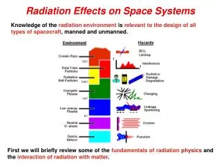
Radiation Effects on Emerging Electronic Materials and Devices • More changes in IC technology and materials in past five years than previous forty years • SiGe, SOI, strained Si, alternative dielectrics, new metallization systems, ultra-small devices… • Future space and defense systems require understanding radiation effects in advanced technologies • Changes in device geometry and materials affect energy deposition, charge collection, circuit upset, parametric degradation…
Team Members • Vanderbilt University • Electrical Engineering: Mike Alles, Dan Fleetwood, Ken Galloway, Marcus Mendenhall, Lloyd Massengill, Robert Reed, Ron Schrimpf, Bob Weller • Physics: Len Feldman, Sok Pantelides • Arizona State University • Electrical Engineering: Hugh Barnaby • University of Florida • Electrical and Computer Engineering: Mark Law, Scott Thompson • Georgia Tech • Electrical and Computer Engineering: John Cressler • North Carolina State University • Physics: Gerry Lucovsky • Rutgers University • Chemistry: Eric Garfunkel, Gennadi Bersuker • Industrial and government collaborators • IBM, Intel, Texas Instruments, Freescale, Jazz, National Semiconductor, SRC/Sematech, Sandia, NASA/DTRA, Lockheed-Martin, Oak Ridge National Lab, CFDRC
Institute for Space and Defense Electronics Resource to support national requirements in radiation effects analysis and rad-hard design Bring academic resources/expertise and real-world engineering to bear on system-driven needs ISDE provides: • Government and industry radiation-effects resource • Modeling and simulation • Design support: rad models, hardening by design • Technology support: assessment, characterization • Flexible staffing driven by project needs • 10 Faculty • 25 Graduate students • 14 Staff and Research Engineers
Schedule—June 14 AM 8:40 MURI Overview Ron Schrimpf, Vanderbilt University 9:00 Overview: Atomic-Scale Theory of Radiation-Induced Phenomena Sokrates Pantelides, Vanderbilt University 9:20 Hf Impurities in Si-SiO2-Si Stacks Apostolos Marinopoulos, Vanderbilt University 9:35 Quantum Mechanical Description of Displacement Damage Formation Matt Beck, Vanderbilt University 9:55 Role of Hydrogen in Radiation Response of Lateral PNP Bipolar Transistors Sasha Batyrev, Vanderbilt University 10:10 Doping-Type Dependence of Damage in Silicon Diodes Dan Fleetwood, Vanderbilt University 10:30 Break 11:00 Defects in Non-Crystalline and Nano-Crystalline Alternative Transition Metal Dielectrics Gerry Lucovsky, North Carolina State University 11:40 Total Dose Response of HfSiON MOS Capacitors Dakai Chen, Vanderbilt University
Schedule—June 14 PM 1:00 Overview: Radiation Effects in Emerging Materials Len Feldman, Vanderbilt University 1:20 Radiation-Induced Charge Trapping in Ultra-Thin HfO2 Based MOSFETs Sriram Dixit, Vanderbilt University 1:40 Radiation Effects in Advanced Gate Stacks Eric Garfunkel, Rutgers University Gennadi Bersuker, Sematech 2:20 Break 2:50 Radiation Effects in SiGe Devices John Cressler, Georgia Tech 3:30 Effects of Angle of Incidence and Temperature on Latchup in 65-nm Technology John Hutson, Vanderbilt University 3:50 Radiation Challenges in Strained Si Technologies Scott Thompson, University of Florida 4:30 Discussion 6:30 Dinner
Schedule—June 15 8:00 Registration and Continental Breakfast 8:30 Total Ionizing Dose Effects in Deep Submicron Bulk CMOS Technologies Hugh Barnaby, Arizona State University 8:50 Band-to-Band Tunneling Induced Leakage Current Enhancement in Irradiated FD-SOI Philippe Adell, JPL 9:10 Enhanced Radiation-Induced Degradation due to Excess Molecular Hydrogen Jie Chen, Arizona State University 9:30 Enabling Radiation-Effects Device Simulations Mark Law, University of Florida 9:50 Overview: Monte Carlo Radiative Energy Deposition Bob Weller, Vanderbilt University 10:10 Impact of Ion Energy and Specie on Single Event Effects Analysis Robert Reed, Vanderbilt University 10:30 Break – High Speed SEE Test Set Demonstration in FGH 310 11:00 Variation in Proton-Induced Energy Deposition in Large Silicon Diode Arrays Christina Howe, Vanderbilt University 11:20 Neutron-Induced Multiple-Bit Upset Alan Tipton and Jonny Pellish, Vanderbilt University 11:40 Effect of Voltage Fluctuations on SET Response of Deep Submicron Digital ICs Matt Gadlage, Vanderbilt University 12:00 Meeting Ends
DURIP-funded High-Speed SEE Test Equipment • DC-40 GHz probe station • 100 nm-step resolution stage • Configure horizontally or vertically • NIR laser irradiation • Broadbeam heavy ion • Eliminates need for high-speed packaging • 12.5 Gbit/s bit error rate tester • 31.5 GHz analog signal generator • 12 GHz real-time digital storage oscilloscope • DC-40 GHz RF coax assemblies • Requires high-speed packaging
Radiation Effects in Emerging Electronic Materials and Devices Approach Motivation • Experimental analysis of state-of-the-art technologies through partnerships with semiconductor manufacturers • Identification of critical mechanisms through first-principles modeling • Implementation and application of a revolutionary multi-scale radiation-effects simulation tool to identify key challenges and develop hardening approaches • More changes in IC technology and materials in past five years than previous forty years—impact on radiation response is dramatic Impact Selected Results • Design tools and methods demonstrated for future rad-hard technologies • Greatly improved error-rate analysis tools allow implementation of more reliable space electronics • First radiation-effects characterization of most advanced technologies (strained Si, HfSiON, etc.)—essential for deployment of state-of-the-art electronics in DoD systems • Development of most accurate rate-prediction tool to date • Identification of tungsten as key rad-effects issue • Fabrication of rad-hard, reliable HfSiON gate dielectrics • Demonstration of extremely rad-hard SiGe technology • First examination of rad effects in strained-Si CMOS
Radiation Effects in Emerging Electronic Materials and Devices: Results Radiation Response of New Materials Impact of New Device Structures • Incorporation of new materials dramatically impacts radiation response • HfO2-based dielectrics and emerging high-k materials tested; HfSiON is very promising • Substrate engineering (strained Si, Si orientations, Si/SiGe, SOI) offers possibility for single-event hardening • New device technologies strongly impact single-event response and TID leakage current • SiGe HBTs, strained Si CMOS, ultra-small bulk CMOS exhibit complicated charge collection mechanisms • Floating-body SOI found to exhibit high radiation-induced off-state leakage due to tunneling Localized Radiation Damage Single Events in New Technologies • RADSAFE—First multi-scale Monte Carlo single-event/rate-prediction tool • Passivation/metallization found to dominate SEE response in some hardened technologies • Excellent agreement with on-orbit data; conventional rate-prediction methods underestimate rate by orders of magnitude • First-principles evidence of micro-melting in small devices • Displacement damage found to depend on substrate doping type • Monte-Carlo simulation tool for non-ionizing energy loss developed
Radiation Effects on Emerging Electronic Materials and Devices: Recent Results New Error-Rate Prediction Tool First Neutron MBU Calculations • Multiple-bit upsets are the key reliability issue in advanced memories • Predicting MBU rate allows design of ECC and memory architecture • Fraction of events resulting in MBUs doubles for grazing angles • Conventional methods underestimate error rate by orders of magnitude • New RADSAFE approach provides outstanding agreement with on-orbit data • Demonstrates that tungsten metallization can dramatically impact error rate First dynamical calculation of displace- ment damage from first principles First Radiation Results on HfSiON • Hf-based dielectrics emerging at 45-nm and below • Much improved radiation response compared to standard Hf silicate films • Interface nitridation is the key to hardness • Very large disordered regions can lead to single-event hard and soft errors • Key reliability issue at 65 nm and below • Possible explanation for dielectric rupture
Radiation Effects on Emerging Electronic Materials and Devices: Recent Results Force Force Z Y X Strain Force Strain Force Effects of Strain on SEE Multiple-Bit Upset • Quantitative analysis of MBU rate in advanced SRAMs • Fraction of events resulting in MBUs increases for new technologies • Explanation of SEE sensitivity of cells resistant to single strikes • First experiments to vary strain during SEE testing planned for 2007 • Strain leads to enhanced mobility and non-isotropic transport • Almost all advanced CMOS will use strain engineering New Gate Dielectrics SEE in SiGe HBTs • Hf-based dielectrics emerging in new technologies • Combined effects of radiation and negative-bias temperature stress much greater than expected • Microbeam testing shows charge collection from distant strikes • Mechanisms identified through simulation • Hardening approach proposed
New Physically-Based Method of Predicting Single-Event Error Rates Sensitive Volumes Materials Transport Calorimetry Circuit Response Cross Section Error Rate Environment (Beam/Natural) TCAD SPICE MRED Circuit Response Transport Calorimetry Sensitive Volumes Materials Locations Dimensions Error Rate Cross Section Solid Model Critical Charge