Download
1 / 1
10 likes | 192 Vues
Development of Front-End Electronics for Picosecond Resolution TOF Detectors Fukun Tang, Enrico Fermi Institute, The University of Chicago

E N D
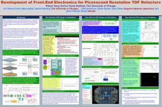
Development of Front-End Electronics for Picosecond Resolution TOF Detectors Fukun Tang, Enrico Fermi Institute, The University of Chicago With Henry Frisch, Mary Heintz, Harold Sanders (The University of Chicago), John Anderson, Karen Byrum, Gary Drake (Argonne National Laboratory) and Jean-Francois Genat (Saclay) Time Stretcher ASIC Design and Simulations Time Stretcher ASIC Design Considerations Introduction Time Stretcher ASIC Design and Simulations Digital Phase-Frequency Detector and Charge Pump Design The Basic Structure of 2GHz PLLs MCP Photo Detector Output Signal Characteristics Withnewly designed 2x2 inches, 1024 equal timing anodes micro-channel plate (MCP) photo detector featuring single pulse rising time in the order of 50ps and transit time spread (TTS) in the order of 25ps, it has become possible to attempt a design of a large area detector with pico-second resolution for relativistic particles. The picosecond Time-of-Flight electronics system consists of a custom ASIC and several commercial chips with a MCP photo-detector that is designed to measure the arrival time of charged particles with a design goal of one picosecond resolution. Effectively, the system acts as a “digital phototube”; all analog signal processing is performed directly by the circuits mounted on the MCP such that the only interfaces that connect to external data collection systems are digital control, digital data output and power supplies. The frond-end ASIC chip will be built with IBM 0.13u SiGe BiCMOS 8HP process. The basic functional circuitry in this chip includes a signal receiver, an ultra low timing jitter/walk discriminator, a control logic block, a 2Ghz PLL common “stop” clock generator and an 1:200 time stretcher with a dynamic range of 1ns. DAQ chip will convert each stretched signals to digital by a 11-bit counter with 200ps resolution. With 1:200 time stretching ratio, the time-to-digital conversion will give 1ps time resolution. Fig. 6 We have designed 2 types of PLLs (Analog and Digital) to ensure if we can achieve a less than 1ps timing jitter for common “stop” clock. Fig.12 Fig. 12 showed digital phase-frequency detector. The proper reset delay time can optimize the phase detector speed and cancel the inherent errors that caused by the glitch from charge pump mismatch and reset signal mismatch when both reference and local clocks arrive in the same time. As a result, the erroneous jitter can be reduced when PLL locked in “zero-phase”. Fig13. is the simplified schematic of charge pump, it is a pair of well matched current steering switches that control the current mirrors that act as PLL’s charge pump. This circuit is operated to minimize the switching charge injection. Fig. 3 MCP Output Signal Fig. 3 shows the simulation result of MCP output signal. The signal rising time is in the order of 15-20ps, pulse width is in the order of 40ps in FWHM. This fast signal requires ASIC to have very high speed circuits to process the front-end analog signal . APLL (Fig.6) is designed fully based on hetero junction transistors, the very high speed and ultra low noise transistors can help achieve very low timing jitter in APLL. The only disadvantage is the narrow pull-in range. Due to the varactor’s variation process-to-process, this may cause VCO’s initial frequency out of the PLL’s pull-in range, in this case, the APLL won’t go to lock. ASIC Technology and Design Kit The DPLL(Fig.7) recently has been designed and simulated. From simulation results, the performance well meets our requirements. The Time Stretcher will be built with IBM 0.13u SiGe BiCMOS 8HP process. This state-of-art SiGe process has the hetero-junction bipolar transistors with the transition frequency as high as 200GHz. The ultra low noise devices allow us to build the very high performance circuits to meet our requirements. Fig. 7 Fig.13 Low Phase Noise VCO Design PLL Lock Range and Jitter Prediction Fig. 14 showed PLL’s locking range. The red chart showed PLL locked to 1.9GHz, blue chart showed PLL locked to 2GHz; the purple chart showed PLL locked to 2.1GHz. A maximum of 10mV ripple was observed in a loop bandwidth of 100MHz, which equivalents to the timing jitter of 0.33ps peak-to-peak. We predict a lower PLL bandwidth can further reduce the ripple. Fig.14 Fig.8 VCO Schematic Fig. 1: MCP’s 1024 anode pads have been grouped to 4 sections, the anode signals in each section will be summed in the equal time anode board and sent to its time stretcher, a DAQ chip converts the stretched pulses from 4 stretchers to digital and also manages the communication with system. Circuit simulation with real time data and interface to other simulation tools Fig. 1 Simulink Modeling and Simulation Due to MCP output signal is in extremely high speed, it is almost impossible to use probe to test and measure real time signals with the circuits. In this case, a complete system simulation is a key factor to build a successful system. Fig. 4 shows the interface between circuit simulation with real time data. Fig.15 A Simulink modeling for fast simulation has been setup, the preliminary simulation results well matched Cadence Spectre simulation. We expect the PLL’s acquisition time can be as long as few hundreds of microseconds or milliseconds if we run PLL in a bandwidth of 100KHz to 1MHz. In this case, it is impossible for Spectre to handle so large transit simulation time scale (miliseconds) with so small resolution time step (few ps). Simulink can be used for the further simulations to optimize the PLL loop bandwidth and loop gains for minimized the PLL jitter. VCO V-F Transfer Function and Phase Noise Fig10: VCO Phase Noise Plot Fig. 4 Stretching Circuit Simulation Fig.16 Fig. 2: The time stretcher receives signal from MCP, a very low timing jitter/walk discriminator will be implemented to generate a “start” signal. The time to measure is the difference between “start” and “Stop”, that is a 500ps-1ns time interval pulse . With the following 1:200 time stretching circuit, a stretched pulse (100n-200ns) then be sent to DAQ chip for digitizing by a 11 bit counter with 200ps resolution. As an evaluation, a preliminary 1:200 time stretching circuit simulation has been done with IHP SiGe SG25H1 process, the current sources with a ratio of 1:200 is in behavior model. Fig. 5 shows 1ns pulse has been stretched to 274ns, the extra 74 ns was caused by the charge injection from the switches. Fig. 9: V-F Transfer Function VCO Layout Fig. 2 Fig. 11: VCO Layout View. Fig. 5: 1:200 pulse stretching pulse Conclusion: (1) IBM 0.13um SiGe BiCMOS8HP has been evaluated, it is very user-friendly design kit. (2) Circuit performance well met to our requirements based on our very low jitter PLL designs. (3) It is possible to generate an on-chip PLL to generate a stable, very low jitter (<1ps) common “stop” clock. (4) More challenging work need to be done on Time Stretcher chip design including the ultra low timing jitter/walk discriminator and the dual-slop ramping time stretching circuits etc. Inductors Varactors Heterojunction Transistors Capacitors 2GHz Phase Locked Loop Design and Simulation 2GHz PLL is required to generate the very low jitter common “stop” clock for Time Stretcher chip. We have simulated analog PLL and digital PLL. The simulation results showed both achieved a timing jitter less than 1ps. The analog PLL uses much less components than digital PLL, but it has very narrow pull-in range, as a result, the initial VCO frequency may out of the PLL’s pull-in range because the VCO varator variations process-to-process. The digital PLL has a very wide locking range and pull-in range, so that the varactor variations process-to-process should not be a problem.