Download
1 / 1
10 likes | 179 Vues
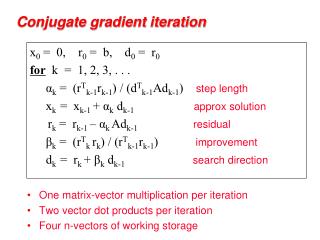
Exploiting Matrix Symmetry to Improve FPGA-Accelerated Conjugate Gradient Jason D. Bakos, Krishna K. Nagar Department of Computer Science and Engineering, University of South Carolina { jbakos, nagar }@cec.sc.edu. Objective: Accelerating Conjugate Gradient Method .

E N D
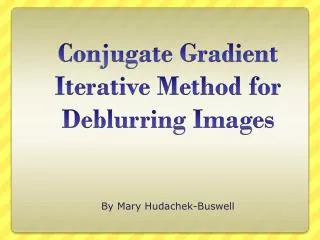
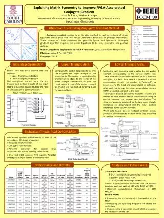
Exploiting Matrix Symmetry to Improve FPGA-Accelerated Conjugate Gradient Jason D. Bakos,Krishna K. Nagar Department of Computer Science and Engineering, University of South Carolina { jbakos, nagar }@cec.sc.edu Objective: Accelerating Conjugate Gradient Method Conjugate gradient method is an iterative method for solving systems of Linear Equations which arise from the Partial Differential Equations of physical phenomena. These systems of Linear Equations are generally Sparse and Symmetric. Conjugate gradient algorithm requires the Linear Equations to be real, symmetric and positive definite. Kernel Computation Implemented on FPGA Coprocessor: Sparse Matrix Vector Multiplication Platform: Virtex-2 Pro 100 FPGA Language: VHDL Advantage Symmetry Upper Triangle Arch. Lower Triangle Arch. Computes the partial dot products for only the diagonal and upper triangle of the input matrix. The vector computed by this architecture is added to the vector of the lower triangle architecture to yield the result vector. A copy of the vector is stored an on-chip in a two-port 64-bit block RAM for each multiplier. Multiplies each incoming matrix value by the vector element corresponding to the current matrix row. These products are accumulated into a BRAM for each multiplier. If a RAW data hazard is detected in either accumulation circuit, the product is “aborted,” by being sent to the host and accumulated in software. After each matrix row, the values accumulated in each BRAM are added and sent to the host. The rows are treated as columns while the columns are treated as rows. Former results in substantial saving of on-chip memory, but requires zero termination. The stream of products produced by the two lower triangle multipliers are accumulated into the result location referenced by the column numbers. When data hazard due to feedback addition occurs, product is directly sent to the host where they are added to the final result vector. • SMVM core has been divided into two sections: • Upper Triangle Architecture • Lower Triangle Architecture • The multipliers process both the top triangle and bottom triangle of the input matrix in parallel: nearly doubles the ratio of computation to communication. • Result = Result upper + Result lower Reduction Circuit: Dual Strided Adder • Two adders operate independently in one of the three states: fill, steady or coalesce. • Requires only two adders • Low buffer requirements • Performs reduction for several rows simultaneously without needing to be flushed. • (nz / row) < 136 increases FIFO capacity, Throttler Circuit pauses input data to prevent overflow Performance and Results Analysis and Future Work • Resource Utilization: • 64/444 18X18 hardware multipliers (14%) • 288/444 block RAMs (64%) • 14075/44096 of the logic slices (15%) • Four double-precision multiplies and six double-precision adds per cycle at 148 MHz: 1480 MFLOPS • Observed computational throughput of 1155 MFLOPS. • Future Work: • Increasing the communication bandwidth to the FPGA • Increasing the operating frequency of adders and multipliers. • Implementing a reduction circuit which overcomes the limitations of the DSA