Nanosilver Technology for Miniaturized Electronics: High-Density Circuits & Modular Construction
210 likes | 273 Vues
Explore the world of nanosilver technology for miniaturized electronics featuring fine-feature conductors, encapsulated components, and stretchable circuitry. This innovative approach allows for quick and cost-effective prototyping, high component density, and rugged design, all while minimizing dead volume and enabling easy subsystem testing. Discover the advantages of embedded nanoparticle silver conductors and how they simplify fabrication processes, reduce layer count, and offer a green, additive approach to circuit design. From wearable sensors to miniature systems utilizing readily available components, this technology offers a versatile and efficient solution for low-volume production and simplified manufacturing scale-up.

Nanosilver Technology for Miniaturized Electronics: High-Density Circuits & Modular Construction
E N D
Presentation Transcript
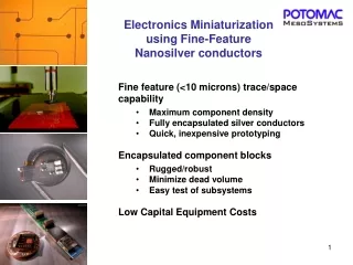
Electronics Miniaturization using Fine-Feature Nanosilver conductors • Fine feature (<10 microns) trace/space capability • Maximum component density • Fully encapsulated silver conductors • Quick, inexpensive prototyping • Encapsulated component blocks • Rugged/robust • Minimize dead volume • Easy test of subsystems • Low Capital Equipment Costs
Nano-silver conductor fabrication Laser ablate channels 1. 1st Squeegee Fill 5. Full oven cure Pulsed UV laser 2. Low T bake 4. Residue removal 3. 2nd Squeegee Fill Conductor resistivity ~ 3X bulk Ag Finished circuit
Embedded nanoparticle silver conductors • Nanoparticle conductor advantages: • Eliminate photolithography • Conductor width limited only by laser focal spot size. • <10 micron trace/space demonstrated • Controllable aspect ratio • Additive, green process Embedded conductor Conventional conductor
Substrates: Polyimide • ABF • LCP • MicroLam • Mylar • Alumina • 15 micron traces • Two sides with via
Stretchable conductors Embedded conductor Polyimide
Quasi-conformal circuitry Sensor MCU Stretchable circuits connect miniature modules • Wearable sensors • Conform to irregular shapes Embedding in elastic polymer 6
High packing density 0201 resistors > 1000 components/cm3 8
Narrow traces reduce layer count and cost Nanosilver • 2 layers • 15 to 30 micron traces • $1000 for first 10 substrates • 1 day turnaround Conventional copper • 4 layers • 75 micron traces • $7800 for first 10 substrates • 12 day turnaround 8 mm 12 mm
Miniature systems using readily available SMT components • Low cost ASIC equivalent • Adaptable to prototyping/low volume production • Simple manufacturing scale-up
Miniature module fabrication • Encapsulate components • Fabricate fine feature interconnects on thin substrates • Nanoparticale silver conductors • Laser direct-write processes • Connect components using conductive adhesives
Component Encapsulation SMD Carrier film Mold Encapsulant Flat surface Exposed pads
Thermal cycling tests -50C to +150C Testing of 50-component Daisy Chains Conductive epoxy Silver traces and pads 0 ohm surface mount resistor -50 C to 150 C 10 minute cycles Microvia Underfill Chain resistance vs time 500 cycles/no failure
Using the modules Solder connection FR4 or Flex 3D stand alone assemblies Miniature subsystems connecting to PCB’s or cables
Body orientation sensor • Accelerometer/magnetometer • Wireless transceiver • Modular construction • Mount on helmet • 20mm x 25mm footprint • Powered by coin cell Radio Programming cable (temporary) MCU/Sensor module
9-axis wireless motion sensor Miniature wireless sensors Radio Sensor module Radio Sensor module Microcontroller Microcontroller Battery Battery
Capital Equipment Required Paste fill & clean station Encapsulation mold Integrated Laser/PnP/Dispense
Capital Equipment NOT required Resist exposure system Etching/Plating tanks Lamination Press Resist stripper
Scaling to higher volume Encapsulation mold Epoxy Dispenser UV laser system Pick and Place Paste fill & clean station
Summary • Highly miniaturized circuits using nanosilver conductors • Simplified design and fabrication • Modular construction • Quick/inexpensive prototyping • Green processes • Minimal capital equipment