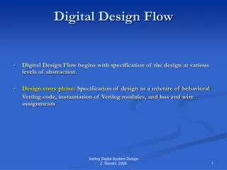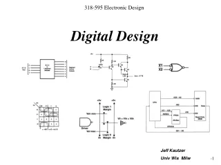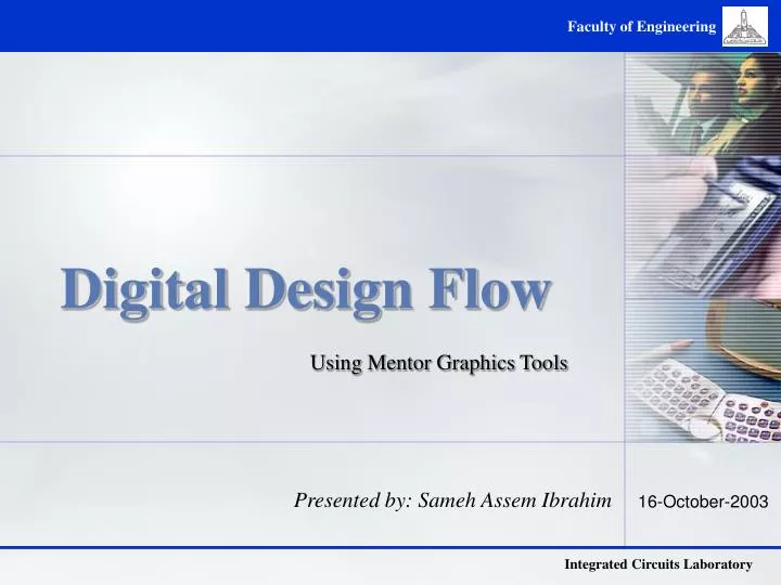

Digital Design Flow
E N D
Presentation Transcript
Digital Design Flow Using Mentor Graphics Tools Presented by: Sameh Assem Ibrahim 16-October-2003
Objectives • Learn the digital design flow starting from VHDL down to physical device verification. • Be familiar with the basics of downloading a design into an FPGA and testing it. • Learn Mentor Graphics Tools: - FPGA Advantage 5.x : - HDL Designer Series (Design Entry) - ModelSim (Simulation) - Leonardo Spectrum (Synthesis) • Learn Xilinx Tools: - ISE Alliance (Placement and Routing) - iMPACT (Design Downloading into FPGA)
Digital Design Flow FPGA ASIC HDL Designer Series (Design Entry) fail ModelSim (VHDL Simulation) VHDL netlist and SDF file for timing simulation VHDL netlist & VITAL Post synthesis verification Leonardo Spectrum (FPGA or ASIC synthesis) Xilinx Alliance (FPGA Implementation) ENIREAD & SG (Format conversion) (Schematic generation) Download design to FPGA chip Design Architect (Schematic editing) fail Testing
Digital Design Flow ASIC DVE (Viewpoints generation) IC station (Autoplace, Autoroute, DRC, LVS, netlist and parasitics extraction) SPICE netlist QuickSim (Digital simulation with delays) Mach TA/PA (Timing and Power analysis) fail GDSII format to foundry
Design Entry • Using HDL Designer Series. • First step is to create a design library. • Design entry can either be Top-Down or Bottom-Up. • Five different design entry methods are available: - VHDL / Verilog - Truth Table - Flow Charts - State Machines - Block Diagrams
Creating the Design Library (1) Run HDL Designer Series: > Start > All Programs > FPGA Advantage 5.x > Design > HDL Designer Design Entry
Creating the Design Library (2) Library Name Library Folder Press OK and Open Library to create designs Design Entry
Creating the Design Design Entry
VHDL Entry (1) Design Entry
VHDL Entry (2) Library Name Entity Name Architecture Name Design Entry
VHDL Entry (3) Save Entity is written here Architecture is written here Design Entry
Truth Table Entry (1) Blue = Input Yellow = Output Right click to add or remove columns Design Entry
Truth Table Entry (2) Save Design Entry Enter required inputs and outputs
Truth Table Entry (3) Architecture Name Library Name Entity Name Yet an entity is still required Design Entry
Truth Table Entry (4) Design Entry
Truth Table Entry (6) Library Name Design Entry Truth Table Entity Name
Truth Table Entry (7) Design Entry
Truth Table Entry (8) Generate HDL Design Entry
Flow Chart Entry Generate HDL Save Flow Stat Point Action End Point An Entity is required Design Entry
State Diagram Entry • Mainly Used for Controllers (Finite State Machines “FSM”) Generate HDL Add state Start state 1st one added Add transition Double click to add action Design Entry Double click to add transition condition
Block Diagram Entry (1) I/O ports Connectors Adding a block (for Top-Down designs) Adding a component (for Bottom-Up designs) Adding a moduleware (a library of VHDL blocks) Block Diagram Editor Design Entry
Block Diagram Entry (2) • Adding a component Browse for your libraries here Browse for your components here Then drag to your Block diagram Design Entry
Block Diagram Entry (3) • Adding a modulware Design Entry
Block Diagram Entry (4) Design Entry Example of a Block Diagram
Test Benches • Test benches are generated automatically as a block diagram with a tester and a block under test. • The tester is a VHDL file with the entity already specified, only the test waveforms are required. Design Entry
Simulation • Using ModelSim. • The created testbench can be used. • Test Waveforms can be created within the program. • Outputs can be checked either as waveforms or as a list of numbers.
Starting ModelSim • Select the design to be simulated and then press • Compilation is done and then ModelSim starts. Simulation
ModelSim Windows Simulation
Using ModelSim (1) Simulation
Using ModelSim (2) Simulation
Using ModelSim (3) Select a signal and either use Force for a specific input or Clock for a periodic signal Simulation
Using ModelSim (4) Run simulation Time of simulation in ns Simulation
Synthesis • Using Leonardo Spectrum. • A technology dependent step. • Either ASICs or FPGAs can be targeted. • Various output formats can be obtained (VHDL/SDF/EDIF)
Running Leonardo Spectrum Click on the synthesizer button Select your design unit Synthesis
Choose what to optimize for and whether to preserve hierarchy or not Choose your device Choose your speed grade Check insert I/0 pads Choose your device family Choose your wiring table Adjusting Synthesis Flow Synthesis
Press Run Flow Generating the EDIF File The EDIF file is created in this path Synthesis
Other Outputs (1) Synthesis RTL Schematic Technology Schematic
Other Outputs (2) VHDL & SDF Area Report Synthesis
Xilinx ISE4.2i Flow • The input to the flow is the EDIF file from Leonardo Spectrum. • The output is a bit file to be downloaded into the FPGA. • Steps are: - Mapping the design blocks into the FPGA design units. - Placement and Rouing of these units. - Genration of the bit file and downloading it to the FPGA. • An FPGA programmer kit must be present, connected to the PC and with a manual at hand to know pins configuration.
Creating a New Project (1) Design Implementation
Creating a New Project (2) Insert the path you want to create the project in Insert the name of the project Add data related to device family, the device itself, and the design flow used Design Implementation
Creating a New Project (3) Choose whether to add the EDIF netlist or to add a copy from it Design Implementation
Implementing the Design There are 3 steps for implementing the design: • Translating the EDIF netlist into primitives. • Mapping these primitives into their technology dependent counterpart. • Placing and routing these technology primitives. Design Implementation
Translating the Design (1) Translates the EDIF and gives a report declaring success of translation or gives warnings and errors. Generates a post translation model that can be in VHDL format for a first step back annotation Design Implementation
Choose VHDL Format Choose properties VHDL File Name Translating the Design (2) Right click on this tab Design Implementation
Mapping the Design Maps the primitives into technology primitives and generates a report. Generates a VHDL as before. Design Implementation
Placement and Routing of the Design Design Implementation
Programming the FPGA Generates the programming bit file for the FPGA Generates a file to be loaded into the PROM (if present in the kit) Downloads the design into the FPGA (iMPACT software) Design Implementation
Thanks • Special thanks go to • Eng. Sameh Talal (Aiat Co.) • Eng. Ahmed Mohsen • For their help in preparing the material for this presentation.