Digital IC Design Flow: A quick look
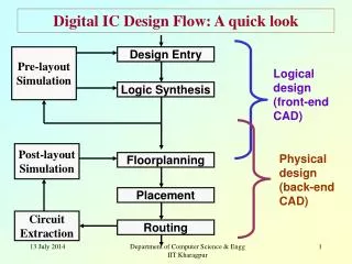
Digital IC Design Flow: A quick look. Pre-layout Simulation. Design Entry. Logical design (front-end CAD). Logic Synthesis. Post-layout Simulation. Physical design (back-end CAD). Floorplanning. Placement. Circuit Extraction. Routing. Design Methodology. VLSI Design Styles.

Digital IC Design Flow: A quick look
E N D
Presentation Transcript
Digital IC Design Flow: A quick look Pre-layout Simulation Design Entry Logical design (front-end CAD) Logic Synthesis Post-layout Simulation Physical design (back-end CAD) Floorplanning Placement Circuit Extraction Routing Department of Computer Science & Engg IIT Kharagpur
Design Methodology Department of Computer Science & Engg IIT Kharagpur
VLSI Design Styles • Programmable Logic Devices • Standard Cell Based Design • Full Custom Design Department of Computer Science & Engg IIT Kharagpur
Programmable Logic Devices Department of Computer Science & Engg IIT Kharagpur
Logic Standard Logic ASIC CPLDs Programmable Logic Device Families Source: Dataquest Common Resources Configurable Logic Blocks (CLB) • Memory Look-Up Table • AND-OR planes • Simple gates Input / Output Blocks (IOB) • Bidirectional, latches, inverters, pullup/pulldowns Interconnect or Routing • Local, internal feedback, and global Programmable Logic Devices (PLDs) Gate Arrays Cell-Based ICs Full Custom ICs SPLDs (PALs) FPGAs Acronyms SPLD = Simple Prog. Logic Device PAL = Prog. Array of Logic CPLD = Complex PLD FPGA = Field Prog. Gate Array Department of Computer Science & Engg IIT Kharagpur
What is FPGA? • Field Programmable Gate Arrays. • Array of logic cells connected via routing channels. • Special I/O cells. • Logic cells are mainly lookup tables (LUT) with associated registers. • Interconnection on SRAM basis or antifuse elements. Department of Computer Science & Engg IIT Kharagpur
Technology and Architecture Tradeoffs • Antifuse elements • High density • Non volatile • Not reprogrammable Department of Computer Science & Engg IIT Kharagpur
Contd. • SRAM cells • Uses more space • Reconfigurable • Volatile, requires PROM Department of Computer Science & Engg IIT Kharagpur
CPLDs and FPGAs CPLD FPGA Complex Programmable Logic Device Field-Programmable Gate Array Architecture PAL/22V10-like Gate array-like More Combinational More Registers + RAM Density Low-to-medium Medium-to-high 0.5-10K logic gates 1K to 500K system gates Performance Predictable timing Application dependent Up to 200 MHz today Up to 135MHz today Department of Computer Science & Engg IIT Kharagpur
CLB CLB Switch Matrix Switch Matrix CLB CLB Xilinx FPGA Routing • 1) Fast Direct Interconnect - CLB to CLB • 2) General Purpose Interconnect - Uses switch matrix Department of Computer Science & Engg IIT Kharagpur
1 2 M1 Technology XC4000 XC4000 XC4000 Design Flow Design Entry in schematic, ABEL, VHDL, and/or Verilog. Vendors include Synopsys, Aldec (Xilinx Foundation), Mentor, Cadence, Viewlogic, and 35 others. Implementation includes Placement & Routing and bitstream generation using Xilinx’s M1 Technology. Also, analyze timing, view layout, and more. Download directly to the Xilinx hardware device(s) with unlimited reconfigurations* !! 3 *XC9500 has 10,000 write/erase cycles Department of Computer Science & Engg IIT Kharagpur
Altera FPGA Family • Altera Flex10K/10KE • LEs (Logic elements) have 4-input LUTS (look-up tables) +1 FF. • Fast Carry Chain between LE’s, cascade chain for logic operations. • Large blocks of SRAM available as well. • Altera Max7000/Max7000A • EEPROM based, very fast (Tpd = 7.5 ns). • Basically a PLD architecture with programmable interconnects. Department of Computer Science & Engg IIT Kharagpur
Gate Array Department of Computer Science & Engg IIT Kharagpur
Standard Cell Based Design Department of Computer Science & Engg IIT Kharagpur
Introduction • One of the most prevalent custom design styles. • Also called semi-custom design style. • Requires development of a full custom mask set. • Basic idea: • All of the commonly used logic cells are developed, characterized, and stored in a standard cell library. • A typical library may contain a few hundred cells including inverters, NAND gates, NOR gates, complex AOI, OAI gates, D-latches, and flip-flops. Department of Computer Science & Engg IIT Kharagpur
Contd. • Each gate type can have multiple implementations to provide adequate driving capability for different fanouts. • For instance, the inverter can have • standard size transistors, • double size transistors, and • quadruple size transistors • The chip designer can choose the proper size to achieve high circuit speed and layout density. Department of Computer Science & Engg IIT Kharagpur
Characteristic of the Cells • Each cell is designed with a fixed height. • To enable automated placement of the cells, and • Routing of inter-cell connections. • A number of cells can be abutted side-by-side to form rows. • The power and ground rails typically run parallel to the upper and lower boundaries of the cell. • Neighboring cells share a common power and ground bus. • nMOS transistors are located closer to the ground rail while the pMOS transistors are placed closer to the power rail. • The input and output pins are located on the upper and lower boundaries of the cell. Department of Computer Science & Engg IIT Kharagpur
Layout of a Typical Standard Cell Department of Computer Science & Engg IIT Kharagpur
Floorplan for Standard Cell Design • Inside the I/O frame which is reserved for I/O cells, the chip area contains rows or columns of standard cells. • Between cell rows are channels for dedicated inter-cell routing. • Over-the-cell routing is also possible. • The physical design and layout of logic cells ensure that • When placed into rows, their heights match. • Neighboring cells can be abutted side-by-side, which provides natural connections for power and ground lines in each row. Department of Computer Science & Engg IIT Kharagpur
Contd. Department of Computer Science & Engg IIT Kharagpur
Contd. • After chip logic design is done using standard cells in the library: • The most challenging task is to place individual cells into rows. • Interconnect them in a way that meets stringent design goals in • circuit speed, • chip area, and • power consumption. • Many advanced CAD tools for place-and-route have been developed and used to achieve the above goals. Department of Computer Science & Engg IIT Kharagpur
Full Custom Design Department of Computer Science & Engg IIT Kharagpur
Introduction • The standard-cells based design is often called semi custom design. • The cells are pre-designed for general use and the same cells are utilized in many different chip designs. • In the full custom design, the entire mask design is done anew without use of any library. • The development cost of such a design style is prohibitively high. • The concept of design reuse is becoming popular in order to reduce design cycle time and cost. Department of Computer Science & Engg IIT Kharagpur
Contd. • The most rigorous full custom design can be the design of a memory cell. • Static or dynamic. • Since the same layout design is replicated, there would not be any alternative to high density memory chip design. • For logic chip design, a good compromise can be achieved by using a combination of different design styles on the same chip. • Standard cells, data-path cells and PLAs. Department of Computer Science & Engg IIT Kharagpur
Contd. • In real full-custom layout in which the geometry, orientation and placement of every transistor is done individually by the designer, • Design productivity is usually very low. • Typically 10 to 20 transistors per day, per designer. • In digital CMOS VLSI, full-custom design is rarely used due to the high labor cost. • Exceptions to this include the design of high-volume products such as memory chips, high-performance microprocessors and FPGA masters. • Next slide shows the full layout of the Intel 486 P chip. • Good example of a hybrid full-custom design. Department of Computer Science & Engg IIT Kharagpur
Department of Computer Science & Engg IIT Kharagpur
Comparison Among Various Design Styles Department of Computer Science & Engg IIT Kharagpur
A Laboratory Flow for Standard Cell Based Design HDL Verilog-XL (Cadence) Logic Simulation SimVision (Cadence) Design Compiler (Synopsys) Synthesis Physical Design Silicon Ensemble (Cadence) Physical Verification Hercules (Avant) Department of Computer Science & Engg IIT Kharagpur
Introduction ToVerilog-HDL Department of Computer Science & Engg IIT Kharagpur
How it started! • Gateway Design Automation • Cadence purchased Gateway in 1989. • Verilog was placed in the public domain. • Open Verilog International (OVI) was created to develop the Verilog Language as IEEE standard. Department of Computer Science & Engg IIT Kharagpur
The Verilog Language • Originally a modeling language for a very efficient event-driven digital logic simulator • Later pushed into use as a specification language for logic synthesis • Now, one of the two most commonly-used languages in digital hardware design (VHDL is the other) • Virtually every chip (FPGA, ASIC, etc.) is designed in part using one of these two languages • Combines structural and behavioral modeling styles Department of Computer Science & Engg IIT Kharagpur
Multiplexer Built From Primitives module mux(f, a, b, sel); output f; input a, b, sel; and g1(f1, a, nsel), g2(f2, b, sel); or g3(f, f1, f2); not g4(nsel, sel); endmodule Verilog programs built from modules Each module has an interface Module may contain structure: instances of primitives and other modules a f1 nsel g1 g4 f g3 b g2 sel f2 Department of Computer Science & Engg IIT Kharagpur
Multiplexer Built From Primitives module mux(f, a, b, sel); output f; input a, b, sel; and g1(f1, a, nsel), g2(f2, b, sel); or g3(f, f1, f2); not g4(nsel, sel); endmodule Identifiers not explicitly defined default to wires a f1 nsel g1 g4 f g3 b g2 sel f2 Department of Computer Science & Engg IIT Kharagpur
Multiplexer Built With Always module mux(f, a, b, sel); output f; input a, b, sel; reg f; always @(a or b or sel) if (sel) f = b; else f = a; endmodule Modules may contain one or more always blocks Sensitivity list contains signals whose change triggers the execution of the block a f b sel Department of Computer Science & Engg IIT Kharagpur
Multiplexer Built With Always module mux(f, a, b, sel); output f; input a, b, sel; reg f; always @(a or b or sel) if (sel) f = b; else f = a; endmodule A reg behaves like memory: holds its value until imperatively assigned otherwise Body of an always block contains traditional imperative code a f b sel Department of Computer Science & Engg IIT Kharagpur
Mux with Continuous Assignment module mux(f, a, b, sel); output f; input a, b, sel; assign f = sel ? b :a; endmodule LHS is always set to the value on the RHS Any change on the right causes re-evaluation a f b sel Department of Computer Science & Engg IIT Kharagpur
Identifiers in Verilog • Any Sequence of letter, digits, dollar sign, underscore. • First character must be a letter or underscore. • It cannot be a dollar sign. • Cannot use characters such as hyphen, brackets, or # in verilog names Department of Computer Science & Engg IIT Kharagpur
Verilog Logic Values • Predefined logic value system or value set : ‘0’, ‘1’ ,’x’ and ‘z’; • ‘x’ means uninitialized or unknown logic value • ‘z’ means high impedance value. Department of Computer Science & Engg IIT Kharagpur
Verilog Data Types • Nets: wire, supply1, supply0 • Registers. • Wire: i) Analogous to a wire in an ASIC. ii) Cannot store or hold a value. • Integer Department of Computer Science & Engg IIT Kharagpur
The Register Data Type • Register Data Type: Comparable to a variable in a programming language. • Default initial value: ‘x’ • module reg_ex1; reg Q; wire D; always @(posedge clk) Q=D; • A reg is not always equivalent to a hardware register, flipflop or latch. • module reg_ex2; // purely combinational reg c; always @(a or b) c=a|b; endmodule Department of Computer Science & Engg IIT Kharagpur
Numbers • Format of integer constants: Width’ radix value; • Verilog keeps track of the sign if it is assigned to an integer or assigned to a parameter. • Once verilog looses sign the designer has to be careful. Department of Computer Science & Engg IIT Kharagpur
Hierarchy • Module interface provides the means to interconnect two verilog modules. • Note that a reg cannot be an input/ inout port. • A module may instantiate other modules. Department of Computer Science & Engg IIT Kharagpur
Instantiating a Module • Instances of module mymod(y, a, b); • Lets instantiate the module, mymod mm1(y1, a1, b1); // Connect-by-position mymod mm2(.a(a2), .b(b2), .y(c2)); // Connect-by-name Department of Computer Science & Engg IIT Kharagpur
Sequential Blocks • Sequential block is a group of statements between a begin and an end. • A sequential block, in an always statement executes repeatedly. • Inside an initial statement, it operates only once. Department of Computer Science & Engg IIT Kharagpur
Procedures • A Procedure is an always or initial statement or a function. • Procedural statements within a sequential block executes concurrently with other procedures. Department of Computer Science & Engg IIT Kharagpur
Assignments • module assignments // continuous assignments always // beginning of a procedure begin //beginning of a sequential block //….Procedural assignments end endmodule • A Continuous assignment assigns a value to a wire like a real gate driving a wire. module holiday_2(sat, sun, weekend); input sat, sun; output weekend; reg weekend; always @(sat or sun) weekend = sat | sun; // Procedural endmodule // assignment module holiday_1(sat, sun, weekend); input sat, sun; output weekend; // Continuous assignment assign weekend = sat | sun; endmodule Department of Computer Science & Engg IIT Kharagpur
Blocking and Nonblocking Assignments • Blocking procedural assignments must be executed before the procedural flow can pass to the subsequent statement. • A Non-blocking procedural assignment is scheduled to occur without blocking the procedural flow to subsequent statements. Department of Computer Science & Engg IIT Kharagpur
Nonblocking Statements are odd! a <= 1; b <= a; c <= b; Nonblocking assignment: a = 1 b = old value of a c = old value of b a = 1; b = a; c = b; Blocking assignment: a = b = c = 1 Department of Computer Science & Engg IIT Kharagpur
Nonblocking Looks Like Latches • RHS of nonblocking taken from latches • RHS of blocking taken from wires a = 1; b = a; c = b; “ a b c ” 1 1 a a <= 1; b <= a; c <= b; “ ” b c Department of Computer Science & Engg IIT Kharagpur
Examples • Non-blocking: always @(A1 or B1 or C1 or M1) begin M1=#3(A1 & B1); Y1= #1(M1|C1); end • Blocking: always @(A2 or B2 or C2 or M2) begin M2<=#3(A2 & B2); Y2<=#1(M1 | C1); end Statement executed at time t causing M1 to be assigned at t+3 Statement executed at time t+3 causing Y1 to be assigned at time t+4 Statement executed at time t causing M2 to be assigned at t+3 Statement executed at time t causing Y2 to be assigned at time t+1. Uses old values. Department of Computer Science & Engg IIT Kharagpur

