Download
1 / 27
280 likes | 580 Vues
Shyue-Kung Lu Department of Electronic Engineering. Digital Systems Design. Syllabus. Recommended Texts 1. Michael D. Ciletti, “Advanced Digital Design with the Verilog HDL,” Prentice Hall ( 新月圖書 ) References

E N D
Shyue-Kung Lu Department of Electronic Engineering Digital Systems Design
Syllabus Recommended Texts 1. Michael D. Ciletti, “Advanced Digital Design with the Verilog HDL,” Prentice Hall (新月圖書) References 1. Richard S. Sandige, “Digital Design Essentials,” Prentice Hall (開發圖書) 2. John F. Wakerly, “Digital Design: Principle and Practices,” Prentice Hall (新月圖書) 3. M. Morris Mano, “Digital Design,” Prentice Hall, Third Edition (滄海書 局,04-27088787) 4. M. Morris Mano, :Digital Logic and Computer Design Fundamentals,” Prentice Hall (新月圖書) Grades 1. 作業 25% 2. 期中考 30 % 3. 期末考 30% 4. Project 15% Project 以歷屆 FPGA 比賽題目為主
Course Overview • Review of combinational and sequential logic design • Introduction to synthesis with HDLs (Verilog HDL) • Programmable logic devices (CPLD and FPGA) • State machines, datapath controllers, RISC CPU • Architectures and algorithms for computation • Synchronization across clock domains • Static Timing Analysis • Fault simulation and testing, JTAG, BIST Digital Systems Design
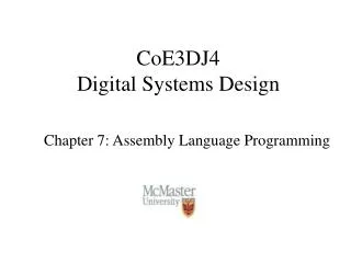
+ out b a Representations of a Digital Design Z = A' •B' •(C + D) = (A' •(B' •(C + D))) Logic expression True table Transistor circuit Gate netlist
Combinational Logic Circuit • Combinational circuit: logic circuit whose outputs at any time are determined directly and only from the present input combination. • A combinational circuit performs a specific information-processing operation fully specified logically by a set of Boolean functions. • Sequential circuit: one that employ memory elements in addition to (combinational) logic gates—their outputs are determined from the present input combination as well as the state of the memory cells.
Combinational Circuit n inputs m outputs Fig. 4-1: Block Diagram of Combinational Circuit Block Diagram of a Combinational Circuit
Combinational Modules • Ripple Carry Adder • Carry Look ahead Adder • Binary Adder-Subtractor • BCD Adder • Magnitude Comparator • Binary Multiplier • Decoder/Encoder • Priority Encoder • Multiplexers/Demultiplexers • Three-State Gates
Characteristic Tables and Equations • Q(t + 1) = D (D Flip-Flop) • Q(t + 1) = JQ’ + K’Q (JK Flip-Flop) • Q(t + 1) = TQ’ + T’Q (T Flip-Flop)
Mealy Machine Outputs dependent on inputs and state variables. Are inputs synchronized with clock?
Input Output State Registers Comb. Circuit Comb. Circuit Outputs dependent on state variables only. Moore Machine
A register is a group of flip-flops, read/written as a unit. A register that goes through a prescribed sequence of states upon the application of input pulses is called a counter. 4-Bit Register
1 0 1 0 I0 I0 0 1 1 0 I0 I0 I0 0 0 1 0 1 I1 I1 0 1 I1 I1 I1 0 0 1 I2 I2 1 0 0 1 1 0 I2 I2 I2 0 1 0 1 0 0 1 I3 I3 I3 I3 I3 0 Register withParallel Load
Shift Register 1 0 1 0 1 1 0 1 0 Edge trigger or level trigger?
No need to go through a sequential logic design process. The flip-flop in the least significant position is complemented with every pulse. A flip-flop in any other position is complemented when all the bits in the lower significant positions are equal to 1. Synchronous Counter