Download
1 / 12
120 likes | 142 Vues
Explore how current flows in a molecule on a silicon substrate, utilizing a coupled DFT-NEGF model for a fully self-consistent solution. Experimental verification aligns with theoretical predictions on isolated and contacted molecular levels.

E N D
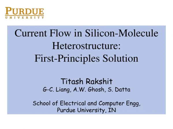
Current Flow in Silicon-Molecule Heterostructure: First-Principles Solution Titash Rakshit G-C. Liang, A.W. Ghosh, S. Datta School of Electrical and Computer Engg, Purdue University, IN
Outline • Qualitative picture: How current flows in a molecule • Example: Molecules on Silicon Substrate: NDR predicted from Band-diagram • Quantitative model: Coupled DFT-NEGF Fully Self-Consistent Solution • Experiments: Agrees with broad features of the theoretical prediction
Isolated Molecular Levels Unoccupied (Conduction-band like) LUMO HOMO Occupied (Valence- band like) Molecules: Isolated (Closed) and Contacted (Open) µ1 Styrene (C8H8) µ2 Broadened Levels Metal Metal
Molecular Levels I-V MolecularLevels n-Silicon p-Silicon Metal Molecular Levels STM STM Metal I-V I-V Ec Ec eV eV Ev Ev ?? V (Silicon) > 0 V (Silicon) < 0 Silicon-Molecule-STM: Negative Diff, Resistance Metal-Molecule-STM: Band-diagram
Self-energy Tunnelgap Silicon STM Molecule (H) Detailed Solution Procedure : Open System, Out-of-equilibrium Molecular Hamiltonian (H) (Density Functional Theory) Self-consistent solution NEGF Converged ?? No Yes Calculate Current
Self-energy , Silicon: Surface States EHT DFT • Ab-initio schemes not useful for Bulk or surface Si • Need for atomistic basis sets for Si -> can be coupled to atomistic molecule • Solution: EHT with Cerda’s parameters Calculated Si Bulk Density of States (DOS) and Si(100) Surface DOS
Self Energy Modeling STM and Vacuum Case I: STM far away from molecule: Effects (i) Electrostatic (ii) Quantum Case II: STM touches the molecule: Collapse of the tunnel barrier EVac EVac Vapp Vapp STM Ec Ec Ev Ev Tunnel Barrier Silicon Mol STM Silicon Mol STM
Electrostatics: Laplace Avg. fraction of bias on molecule Tunnelgap Silicon STM Styrene Vmol Vsi Vair
Fully Self-Consistent I-V Ab-initio fully self-consistent I-V of Styrene on p-Si(100): LDA/6-31g(d), 163x163
Molecule on n-type Si(100) Molecule on p-type Si(100) 5.00E-09 0.6 4.00E-09 NDR 0.5 3.00E-09 0.4 0.3 2.00E-09 0.2 1.00E-09 I (nA) 0.1 0.00E+00 0 -6 -4 -2 0 2 4 6 -6.0 -4.0 -2.0 0.0 2.0 4.0 6.0 -1.00E-09 -0.1 -2.00E-09 -0.2 -0.3 -3.00E-09 V (Volts) NDR -4.00E-09 Mark Hersam Group (Northwestern University) Nanoletters, 01/04 Cover story Experimental Verification
Summary and Conclusions 1. General Framework of coupled DFT-NEGF self-consistent solution 2. Novel RTD proposed for a Molecule-Silicon Heterostructure: polarity reversal predicted dependent on type of doping 3. Experiments agree with the broad feature of polarity reversal, however the exact location of NDR peaks on n-type substrates remain to be understood