Download
1 / 46
560 likes | 1.38k Vues
Carbon Nanotubes: The exciting future of fullerenes. http://www.futuretimeline.net/subject/nanotechnology.htm. Papers used: “Carbon Nanotubes: Present and Future Commercial Applications “ “Single-Wall Carbon Nanotubes” “ Carbon nanotube mass production: principles and processes ”

E N D
Carbon Nanotubes: The exciting future of fullerenes http://www.futuretimeline.net/subject/nanotechnology.htm Papers used: “Carbon Nanotubes: Present and Future Commercial Applications “ “Single-Wall Carbon Nanotubes” “Carbon nanotube mass production: principles and processes” “Fabrication and multifunctional properties of a hybrid laminate with aligned carbon nanotubes grown in situ” • Presented By: • David Chaar • Steven Hering • Phillip Thane • KoriMondin
ABSTRACT Currently CNT’s are used in specialty applications such as bikes, boats, and race cars because of CNT’s very light weight compared to competing high strength materials. Most recently CNT’s have been used in batteries, transistors, and even as a shield against space debris for NASA’s Juno spacecraft. http://www.sciencemag.org.lib-ezproxy.tamu.edu:2048/content/339/6119/535.full.pdf The increasing demand for CNT’s is driving advances in CNT synthesis, purification, and chemical modification technology. The advances in production are beginning to create new applications for CNT’s that go beyond the incorporation of bulk powders. The most promising areas of research are microelectronics, biotechnology, water purification, and composite materials.
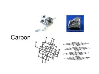
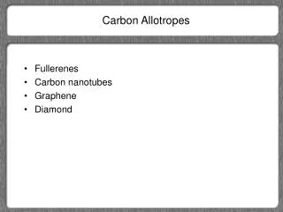
Introduction • Carbon nanotubes • layers of carbon bonded in hexagonal lattices • form large sheets of graphene • when sheets are rolled up they form tubes which are existent at a nanometer scale http://4.bp.blogspot.com/JT5P-RJi06I/TF-lJcmNGmI/AAAAAAAAAFQ/ulIUwi-8lMc/s1600/CNT.gif http://journalclubscienceblog.files.wordpress.com/2012/07/multiwall-carbon-nanotube.jpg • Two types of CNTs • multi walled • make incredibly strong fibers • single walled • well suited for electrical and thermal conduction • the strength of a MWNT is ten times higher than any other known fiber!
Properties stem from “graphene” • Conducting properties determined by nature of electronic states near Fermi energy • energy of highest occupied electronic state at zero temperature • Band structure • Unlike metal or semiconductor • In between • Most directions, electrons at Fermi energy are backscattered by atoms in the lattice • Other directions, electrons that scatter from different atoms in lattice interfere destructively and suppresses backscattering • Only happens in y direction and directions 60°, 120°, 180°, 240° from y Electron Structure of Nanotubes http://www.physics.umd.edu/condmat/mfuhrer/publications/PWorld00all.pdf
Electron Structure of Nanotubes • Converting 2-D to 1-D forms tube • Resulting boundary conditions on wavefunction quantizes kn, component of k perpendicular to axis of tube • kn =2πn/C • Tube axis in y direction: tube acts as 1-D metal • Tube axis in different direction: semiconducting 1-D band structure • Converting from 2D to 1D • simply a matter of changing the tube orientation • usually done with an electrical current • If CNT is turned such that the axis is pointing in the metallic direction it results in a tube whose dispersion is a slice through the center of a cone. The reason it's called 1D at that point is because the fermi velocity is comparable to typical metals. http://www.physics.umd.edu/condmat/mfuhrer/publications/PWorld00all.pdf
Nanotubes: how they conduct • Attach metal electrodes • Can be connected to single tube or bundle of several hundred tubes • Drop tubes onto electrodes (a) • Deposit tubes on substrate, locate with scanning electron microscope, attach leads to tubes using lithography (b) • Advanced techniques • Growing tubes between electrodes • Attaching tubes to surface in controllable fashion using electrostatic or chemical forces • Source and drain allow conducting properties to be measured a b http://www.physics.umd.edu/condmat/mfuhrer/publications/PWorld00all.pdf http://www.physics.umd.edu/condmat/mfuhrer/publications/PWorld00all.pdf
Nanotubes: how they conduct • Gate used to electrostatically induce carriers into tube • Negative bias on gate induces positive charges on tube • Positive bias induces negative charges • Conductance of tube measured as function of gate voltage http://www.physics.umd.edu/condmat/mfuhrer/publications/PWorld00all.pdf
CNT Synthesis http://www.readcube.com/articles/10.1038/nnano.2009.67 • Chemical vapor deposition • Most commonly used method of high volume CNT production • A catalyst is placed in a reactor and carbon containing gas is pumped through at a specific temperature and pressure so that it forms graphene on the surface of the catalyst • Current bulk production methods • leave a large number of impurities and contaminants • must be washed out with chemical treatments • can reduce CNT length and cause defects in CNT sidewalls
Product Chemical vapor deposition creates a bulk powder of CNT’s. Currently research is being done to find how catalyst and production conditions influence CNT chirality, diameter, length, and purity. Post Production Processing: High purity SWNT powders are created by separating bulk powder by density or gel chromatography. Following this various washes and thermal treatments are used to create stability on the CNT surface by addition of surfactants. Bulk CNT Powder http://farm4.static.flickr.com/3186/3115816442_f5e050a423.jpg?v=0 Separation of three proteins by gel chromatography. In the same way, CNT’s can be separated based on density. http://www.imb-jena.de/~rake/Bioinformatics_WEB/gifs/gel_filtration2.gif
CNT Production: Bottom-line • Laser Alignment • Using lasers, single walled carbon nanotubes can be synthesized with large lengths, if this process can be scaled up then the cost of processing and purifying bulk powders to achieve desirable lengths could be avoided. • Self Aligning Growth • Synthesis of long CNT’s could be done without expensive and time consuming liquid processing by coating substrates with catalyst particles which cause the CNT’s to line up together as they grow. http://newsroom.unl.edu/releases/downloadables/photo/20090225nanotubes.jpg http://ars.els-cdn.com/content/image/1-s2.0-S0925400512002213-gr7.jpg
Composite Materials • Electrically conductive fillers in plastics • CNT powders mixed with polymers • Increase stiffness, strength, toughness • No compromise in mechanical properties • CNT resins • Enhance fiber composites • Wind turbines, boat hulls http://www.sciencemag.org.lib-ezproxy.tamu.edu:2048/content/339/6119/535.full.pdf
Composite Materials • MWNT added as flame retardant additives to plastics • Change in rheology by nanotube loading • Yarn • High surface area increases strength when knotted http://www.sciencemag.org.lib-ezproxy.tamu.edu:2048/content/339/6119/535.full.pdf
Work performed – CNT synthesis (MWNT) • Use of Fluidized bed reactors for CVD • Allows for uniform gas diffusion • Allows for heat transfer to metal catalyst nanoparticles • Has allowed for factors to greatly decrease MWNT commercial prices • Scale-up • Use of low cost feed stocks • Increase in yields http://en.wikipedia.org/wiki/File:Fluidized_Bed_Reactor_Graphic.svg
Work performed – CNT synthesis (SWNT) • SWNT synthesis by CVD requires • Separation according to chirality by density gradient centrifugation + surfactant wrapping or gel chromatography • Stable CNT suspensions will require addition of surfactant • Washing or thermal treatment needed to remove surfactant • Very tight process control SWNT >> MWNT http://cleanoceanaction.blogspot.com/2011/07/save-money-and-ocean.html http://www.customtimberloghomes.com/log-home-cost-vs-timber-home-cost
Work performed – CNT synthesis • Synthesis of long, aligned CNTs • Preferably without requiring to disperse in a liquid • Methods include • Self-aligned growth of horizontal & vertical CNTS on substrates • Substrates are coated with catalyst particles http://www.elec.york.ac.uk/research/projects/Carbon_Nanotube_Growth_and_Characterization.html
Work performed – CNT synthesis • Can synthesize CNT forests and manipulate into • Thin films • Intricate 3D microarchitectures • Directly spun into long yarns • Drawn into sheets http://www.ornl.gov/info/ornlreview/v38_3_05/article11.shtml http://www.imec.be/ScientificReport/SR2011/1414173.html
Work performed – Composite Materials • To organize CNTs at a large scale, fiber composites are created by growing aligned CNT forests on • Glass • SiC • Alumina • Carbon Fibers • Creates fuzzy fibers • Improves toughness by more than 50% http://cosmiclog.nbcnews.com/_nv/more/section/archive?year=2011&month=1&ct=a&pc=25&sp=25
Work performed – Coating and Films • CNT can be a multifunctional coating material • Leveraging CNT dispersion • Functionalization • Large-area deposition techniques • Example: • MWNT containing paints reduce bio-fouling on hulls • Anticorrosion coating on metals while providing stiffness and strength http://marinesupplydock.wordpress.com/2012/10/25/a-winterization-guide-for-boats/
Work performed – Coating and Films • CNT-based transparent conducting films • Alternative to expensive indium tin oxide (ITO) • Flexible, and not brittle • Application in • Displays • Touch screen devices • photovolatics http://en.wikipedia.org/wiki/File:Samsung_flexible_AMOLED_phone.jpg
Work performed – Coating and Films • CNT conductors can be deposited from solution • Slot-die coating • Ultrasonic spraying • Can be patterned by economic nonlithographic methods • Recent developments have allowed for • SWNT films with 90% transparency • Sheet resistivity of 100 ohm per square • Adequate applications such as CNT thin-film heaters like defrosting windows or sidewalks http://funnypicturesplus.com/defrosting-car-window.html
Work performed – Microelectronics • SWNTs are attractive for transistors due to • Low electron scattering • Band-gap • Depends on diameter • Depends on chiral angle • Also compatible with field-effect transistor (FET) architectures and high k-dielectrics. • Current densities achieved were greater than those obtained for Si devices. http://www.circuitstoday.com/fet-field-effect-transistors-introduction
Work performed – Microelectronics • CNT arrays containing 10-103 SWNTs in patterned films increases • Output current • Compensates for defects and chirality differences • Improves device uniformity and reproducibility • Up to 105 CNTs on a single chip http://www.nanotech-now.com/news.cgi?story_id=06788
Work performed – Microelectronics • CNT thin film transistors (TFT) appealing for organic light emitting diodes (OLED) displays • Higher mobility than amorphous Si • Can be deposited at low T, and non-vacuum methods http://www.sciencemag.org/content/339/6119/535/F3.large.jpg http://http://www.charterworld.com/news/new-sony-flexible-oled-display-rollable-around-a-pencil-to-have-applications-in-the-superyacht-industry/oled-display
Work performed – Microelectronics • CNTs can replace Cu in microelectronic interconnects. • Low scatter • High current carrying capacity • Resistance to electromigration • CNTs can be used in high-power amplifiers and function as both • Electric leads • Heat dissipaters http://www.sciencemag.org/content/339/6119/535/F3.large.jpg
Work performed – Energy Storage • Use of MWNTs in Li-ion batteries • Laptop notebooks • Mobile phones • MWNT powder blended with active materials • Increases electrical connectivity • Increases mechanical strength • Enhances cycle life and rate capability http://metaefficient.com/computers/the-greenest-notebook-computers-of-2008.html
Work performed – Energy Storage (supercapacitors) • Study on packaged cells utilizing forest-grown SWNTs revealed remarkable performance • 16 Wh kg-1 energy density • 10 kW kg-1 power density • 16 year lifetime forecast • The only drawback is the high cost of SWNTs http://www.sciencemag.org/content/339/6119/535/F3.large.jpg
Work performed – Energy Storage (Fuel Cells) • Use of CNTs in fuel cells as catalyst • Reduce Pt usage by 60% • For organic solar cells, CNTs • Reduce undesired carrier recombination • Enhance resistance to photo-oxidation http://www.sciencemag.org/content/339/6119/535/F3.large.jpg
Work performed – Environment (Water filters) • Application of tangled CNT sheets to provide robust networks that have controlled nanoscale porosity and are robust • Mechanically • Electrochemically • Used to electrochemically oxidize organic contaminants, viruses, and bacteria • Enhanced permeability will enable lower energy cost for water desalination http://www.sciencemag.org/content/339/6119/535/F3.large.jpg
Work performed – Biotechnology • CNTs have been investigated as components of • Biosensors • Medical devices • Appeal due to compatibility with biomolecules (DNA/proteins) from two aspects: • Dimensional • chemical http://convergence.ucsb.edu/news/ultra-sensitive-electrical-biosensor-unlocks-potential-instant-diagnostic-devices
Work performed – Biotechnology • CNTs enable biological functions like • Fluoroscence • Photoacoustic imaging • Localized heating via near-infrared radiation http://en.wikipedia.org/wiki/File:FluorescentCells.jpg
Work performed – Biotechnology (SWNT biosensors) • Adsorption of target molecules on CNT surface allow for large changes in • Electrical impedance • Optical properties • Application include • Gas and toxin detection in industry and military • Test strips for hormones and biological markers (NO2,troponin, estrogen, progesterone) http://bme240.eng.uci.edu/students/08s/jentel/Diagnose-hereditary-disease.htm
Work performed – Biotechnology (In vivo) • CNT can be loaded with cargo on walls or inside tube • Attaches to cell membrane • Release cargo upon near-infrared radiation http://thepluripotent.com/?tag=cirm
Nanotube transistors • Semiconducting nanotubes • Tube turned on: negative bias to gate • Induces holes on tube • Makes conductive • Tube turned off: positive bias to gate • Depletes holes • Decreases conductance • Resistance of off state can be more than million times greater than on state • similar to p-type metal-oxide-silicon field effect transistor http://www.physics.umd.edu/condmat/mfuhrer/publications/PWorld00all.pdf
Nanotube transistors • Conductance limited by barriers that holes see as they traverse tube • Barriers caused by • structural defects in tube • Atoms absorbed on tube • Localized charges near tube • Holes see peaks and valleys that they must hop through if tube is to conduct • Resistance dominated by highest barriers http://www.physics.umd.edu/condmat/mfuhrer/publications/PWorld00all.pdf
Nanotubes as one-dimensional metals • Have large number of carriers • Conductance much larger than semiconducting nanotubes • Conductance oscillates as function of gate voltage • Oscillations occur when additional electron is added to nanotube • Regular and periodic oscillations: electronic states extended along entire length of tube • Electrons can travel long distances in nanotubes without being backscattered http://www.physics.umd.edu/condmat/mfuhrer/publications/PWorld00all.pdf
Nanotubes as one-dimensional metals • 1-D conductor at low voltage makes it ideal system to test ideas about electrons • 1-D repulsive Coulomb interactions between neighboring electrons should behave differently than 2-D or 3-D • 2-D/3-D (a) • Behaves as Fermi Liquid • Electrons fill low energy states up to Fermi energy • Low energy excitations act like free electrons (can tunnel without difficulty) • 1-D (b) • Low energy excitations are collective excitations of entire electron system http://www.physics.umd.edu/condmat/mfuhrer/publications/PWorld00all.pdf
New Devices and Geometries • Crossing metallic and semiconducting tube • Metallic tube locally depletes holes in semiconducting tube • Electron travelling tube must overcome barrier • Applying voltage at one end of tube leads to correction at that end but not other • Nanotube coils • Individual tube loops back on itself to form ring-like structure • Used as solenoids to create magnetic fields or study quantum interference phenomena http://www.physics.umd.edu/condmat/mfuhrer/publications/PWorld00all.pdf
Future Works • Investigate why yarns and sheets have thermal, electrical, and mechanical properties that are significantly lower than individual CNT. http://www.fastcompany.com/3000082/creating-artificial-muscles-more-powerful-anything-nature http://www.gaia3d.co.uk/3d-models/3d-chemistry/carbon-nanotube/
Future Works • Better understand CVP process condition • Reduce contaminants • Avoid costly thermal annealing and chemical treatments http://www.made-in-zelenograd.com/products/mvu-tm-izophase-cvd-icp/
Future Works • Better understand how CVP process conditions effect • Chirality • Diameter • Length • Purity http://drugdeliverysystems.webs.com/nanotubes.htm
Future Works • Further price reductions of SWNT needed • Commercial application of SWNT is emerging • Applications require chiral-specific SWNTs • Synthesize long aligned CNTs without the need to disperse in a liquid http://nextbigfuture.com/2010/11/emerging-applications-of-carbon.html http://drugdeliverysystems.webs.com/nanotubes.htm
Future Works • Improve resistivity of transparent SWNT films so that they are better than equally transparent, optimally doped ITO coatings. http://www.tradekorea.com/products/ito_coating_glass.html http://onlinelibrary.wiley.com/doi/10.1002/smll.201201398/abstract
Future Works • Difficult control of CNT • Diameter • Chirality • Density • placement • Introduces difficulty to control microelectronic production over large areas. • Required improved understanding of CNT surface chemistry for better commercialization of CNT TFT http://www.mikroe.com/old/books/keu/04.htm
Future Works • CNT biotoxicity • Must control CNT retention within body • Prevent undesirable accumulation • Better understand surface chemistry and geometry • Medical application requires better understanding of interaction of CNT with the immune system • Develop exposure standards for • Inhalation • Ingestion • Skin contact • Injection http://hyperphysics.phy-astr.gsu.edu/hbase/biology/celmem.html
Conclusions Films Biotechnology Energy storage Coating Microelectronics Water filters Transistors Biosensors screens Environment http://4.bp.blogspot.com/_JT5P-RJi06I/TF-lJcmNGmI/AAAAAAAAAFQ/ulIUwi-8lMc/s1600/CNT.gif
References M.F.L De Volder, S.H. Tawfick, R.H. Baughman, A.J Hart, Carbon Nanotubes: Present and Future Commercial Applications. Science 339, 6119 (2013) P.L McEuen, Single-wall carbon nanotubes. Physics World 13, 6 (2000). Q. Zhang, J.-Q. Huang, M.-Q. Zhao, W.-Z. Qian, F. Wei, Carbon nanotube mass production: principles and processes. ChemSusChem4, 864 (2011). E. J. Garcia, B. L. Wardle, A. J. Hart, N. Yamamoto, Fabrication and multifunctional properties of a hybrid laminate with aligned carbon nanotubes grown In Situ. Compos. Sci. Technol. 68, 2034 (2008). http://research.che.tamu.edu/groups/Seminario/index-1.html