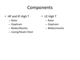
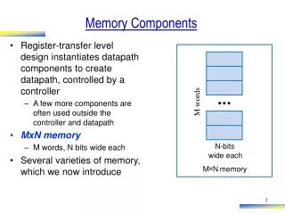
Memory Components
N-bits. wide each. Memory Components. Register-transfer level design instantiates datapath components to create datapath, controlled by a controller A few more components are often used outside the controller and datapath MxN memory M words, N bits wide each

Memory Components
E N D
Presentation Transcript
N-bits wide each Memory Components • Register-transfer level design instantiates datapath components to create datapath, controlled by a controller • A few more components are often used outside the controller and datapath • MxN memory • M words, N bits wide each • Several varieties of memory, which we now introduce M words × M N memory
32 32 W_data R_data 4 4 W_addr R_addr W_en R_en × 16 32 register file Random Access Memory (RAM) • RAM – Readable and writable memory • “Random access memory” • Strange name – Created several decades ago to contrast with sequentially-accessed storage like tape drives • Logically same as register file – Memory with address inputs, data inputs/outputs, and control • RAM usually just one port; register file usually two or more • RAM vs. register file • RAM typically larger than roughly 512 or 1024 words • RAM typically stores bits using a bit storage approach that is more efficient than a flip flop • RAM typically implemented on a chip in a square rather than rectangular shape – keeps longest wires (hence delay) short Register file from Chpt. 4 32 data 10 addr × 1024 32 r w R A M en RAM block symbol
32 data 10 addr 1024x32 bit storage word r w RAM block enable en d0 (aka “cell”) a0 w o r d a1 AxM d1 decoder data cell a(A-1) word word d(M-1) e enable enable r w data RAM cell RAM Internal Structure • Similar internal structure as register file • Decoder enables appropriate word based on address inputs • rw controls whether cell is written or read • Let’s see what’s inside each RAM cell wdata(N-1) wdata(N-2) wdata0 Let A = log2M addr0 addr1 addr addr(A-1) clk en r w to all cells rdata(N-1) rdata(N-2) rdata0
32 data 10 addr 1024x32 r w RAM en SRAM cell data data’ 1 0 d 1 0 1 word enable data data’ cell d 1 d’ 0 0 word enable Static RAM (SRAM) SRAM cell • “Static” RAM cell • 6 transistors (recall inverter is 2 transistors) • Writing this cell • word enable input comes from decoder • When 0, value d loops around inverters • That loop is where a bit stays stored • When 1, the data bit value enters the loop • data is the bit to be stored in this cell • data’ enters on other side • Example shows a “1” being written into cell data data’ cell d d’ a 0 word enable a a
32 data 10 addr 1024x32 r w RAM en 1 1 1 <1 1 Static RAM (SRAM) • “Static” RAM cell • Reading this cell • Somewhat trickier • When rw set to read, the RAM logic sets both data and data’ to 1 • The stored bit d will pull either the left line or the right bit down slightly below 1 • “Sense amplifiers” detect which side is slightly pulled down • The electrical description of SRAM is really beyond our scope – just general idea here, mainly to contrast with DRAM... SRAM cell data data’ d 1 0 a word enable To sense amplifiers
32 data 10 addr 1024x32 r w RAM en Dynamic RAM (DRAM) • “Dynamic” RAM cell • 1 transistor (rather than 6) • Relies on large capacitor to store bit • Write: Transistor conducts, data voltage level gets stored on top plate of capacitor • Read: Just look at value of d • Problem: Capacitor discharges over time • Must “refresh” regularly, by reading d and then writing it right back DRAM cell data c ell word enable d capacitor slowly discharging ( a ) data enable discharges d ( b )
Comparing Memory Types • Register file • Fastest • But biggest size • SRAM • Fast • More compact than register file • DRAM • Slowest • And refreshing takes time • But very compact • Use register file for small items, SRAM for large items, and DRAM for huge items • Note: DRAM’s big capacitor requires a special chip design process, so DRAM is often a separate chip MxN Memory implemented as a: register file SRAM DRAM Size comparison for same number of bits (not to scale)
RAM Example: Digital Sound Recorder • Behavior • Record: Digitize sound, store as series of 4096 12-bit digital values in RAM • We’ll use a 4096x16 RAM (12-bit wide RAM not common) • Play back later • Common behavior in telephone answering machine, toys, voice recorders • To record, processor should read a-to-d, store read values into successive RAM words • To play, processor should read successive RAM words and enable d-to-a
4096x16 RAM 16 analog-to- digital-to- 12 digital analog ad_buf Ra Rw Ren converter converter ad_ld da_ld processor Local register: a (12 bits) a<4095 S T a=0 ad_ld=1 ad_buf=1 U Ra=a Rrw=1 a=a+1 Ren=1 a=4095 RAM Example: Digital Sound Recorder • RTL design of processor • Create high-level state machine • Begin with the record behavior • Keep local register a • Stores current address, ranges from 0 to 4095 (thus need 12 bits) • Create state machine that counts from 0 to 4095using a • For each a • Read analog-to-digital conv. • ad_ld=1, ad_buf=1 • Write to RAM at address a • Ra=a, Rrw=1, Ren=1 Record behavior a
4096x16 RAM 16 analog-to- digital-to- 12 digital analog ad_buf Ra Rw Ren converter converter ad_ld da_ld processor Local register: a (12 bits) a<4095 V W a=0 ad_buf=0 Ra=a X Rrw=0 Ren=1 a=a+1 a=4095 RAM Example: Digital Sound Recorder • Now create play behavior • Use local register a again, create state machine that counts from 0 to 4095 again • For each a • Read RAM • Write to digital-to-analog conv. • Note: Must write d-to-a one cycle after reading RAM, when the read data is available on the data bus • The record and play state machines would be parts of a larger state machine controlled by signals that determine when to record or play data bus Play behavior a da_ld=1
32 data 10 addr × 1024 32 r w R A M en RAM block symbol 32 data 10 1024x32 addr ROM en ROM block symbol Read-Only Memory – ROM • Memory that can only be read from, not written to • Data lines are output only • No need for rw input • Advantages over RAM • Compact: May be smaller • Nonvolatile: Saves bits even if power supply is turned off • Speed: May be faster (especially than DRAM) • Low power: Doesn’t need power supply to save bits, so can extend battery life • Choose ROM over RAM if stored data won’t change (or won’t change often) • For example, a table of Celsius to Fahrenheit conversions in a digital thermometer
32 data 10 1024x32 addr ROM en ROM block symbol Read-Only Memory – ROM • Internal logical structure similar to RAM, without the data input lines Let A = log2M bit storage word block enable d0 (aka “cell”) a0 w o r d addr0 a1 addr1 AxM d1 decoder data addr addr(A-1) a(A-1) word word d(M-1) e enable enable clk data en ROM cell rdata(N-1) rdata(N-2) rdata0
ROM Types • If a ROM can only be read, how are the stored bits stored in the first place? • Storing bits in a ROM known as programming • Several methods • Mask-programmed ROM • Bits are hardwired as 0s or 1s during chip manufacturing • 2-bit word on right stores “10” • word enable (from decoder) simply passes the hardwired value through transistor • Notice how compact, and fast, this memory would be 1 data line 0 data line cell cell word enable
blown fuse ROM Types • Fuse-Based Programmable ROM • Each cell has a fuse • A special device, known as a programmer, blows certain fuses (using higher-than-normal voltage) • Those cells will be read as 0s (involving some special electronics) • Cells with unblown fuses will be read as 1s • 2-bit word on right stores “10” • Also known as One-Time Programmable (OTP)ROM 1 data line 1 data line cell cell a word enable fuse
ROM Types • Erasable Programmable ROM (EPROM) • Uses “floating-gate transistor” in each cell • Special programmer device uses higher-than-normal voltage to cause electrons to tunnel into the gate • Electrons become trapped in the gate • Only done for cells that should store 0 • Other cells (without electrons trapped in gate) will be 1 • 2-bit word on right stores “10” • Details beyond our scope – just general idea is necessary here • To erase, shine ultraviolet light onto chip • Gives trapped electrons energy to escape • Requires chip package to have window data line data line floating-gate transistor c ell c ell 1 0 or t word Ð Ð e e ting enable a r e t t a trapped electrons g
32 data 10 addr 1024x32 en EEPROM write busy ROM Types • Electronically-Erasable Programmable ROM (EEPROM) • Similar to EPROM • Uses floating-gate transistor, electronic programming to trap electrons in certain cells • But erasing done electronically, not using UV light • Erasing done one word at a time • Flash memory • Like EEPROM, but all words (or large blocks of words) can be erased simultaneously • Become common relatively recently (late 1990s) • Both types are in-system programmable • Can be programmed with new stored bits while in the system in which the ROM operates • Requires bi-directional data lines, and write control input • Also need busy output to indicate that erasing is in progress – erasing takes some time or t ting a r e t t a g
“Hello there!” ROM Example: Talking Doll “Hello there!” audio divided into 4096 samples, stored in ROM • Doll plays prerecorded message, trigger by vibration • Message must be stored without power supply Use a ROM, not a RAM, because ROM is nonvolatile • And because message will never change, use a mask-programmed ROM or OTP ROM • Processor should wait for vibration (v=1), then read words 0 to 4095 from the ROM, writing each to the d-to-a speaker 4096x16 ROM “Hello there!” a d 16 a digital-to- analog vibration Ra Ren converter sensor da_ld processor
4096x16 ROM R a=a 16 digital-to- R en=1 analog Ra Ren converter da_ld processor v ROM Example: Talking Doll • High-level state machine • Create state machine that waits for v=1, and then counts from 0 to 4095 using a local register a • For each a, read ROM, write to digital-to-analog converter Local register: a (12 bits) v a<4095 a=0 S T a d a U v’ da_ld=1 a=4095 a=a+1
4096x16 Flash busy 16 analog-to- 12 digital digital-to- ad_buf Ra er bu Rrw Ren converter analog converter ad_ld processor da_ld rec record play microphone speaker ROM Example: Digital Telephone Answering Machine Using a Flash Memory • Want to record the outgoing announcement • When rec=1, record digitized sound in locations 0 to 4095 • When play=1, play those stored sounds to digital-to-analog converter • What type of memory? • Should store without power supply – ROM, not RAM • Should be in-system programmable – EEPROM or Flash, not EPROM, OTP ROM, or mask-programmed ROM • Will always erase entire memory when reprogramming – Flash better than EEPROM “We’re not home.”
4096x16 Flash 16 analog-to- 12 digital digital-to- ad_buf Ra er bu Rrw Ren converter analog converter ad_ld processor da_ld rec record play microphone speaker Local register: a (13 bits) bu a<4096 S T U bu’ a=0 er=0 ad_ld=1 er=1 ad_buf=1 V Ra=a r ec Rrw=1 Ren=1 a=4096 a=a+1 ROM Example: Digital Telephone Answering Machine Using a Flash Memory • High-level state machine • Once rec=1, begin erasing flash by setting er=1 • Wait for flash to finish erasing by waiting for bu=0 • Execute loop that sets local register a from 0 to 4095, reading analog-to-digital converter and writing to flash for each a a w d r en a
Blurring of Distinction Between ROM and RAM • We said that • RAM is readable and writable • ROM is read-only • But some ROMs act almost like RAMs • EEPROM and Flash are in-system programmable • Essentially means that writes are slow • Also, number of writes may be limited (perhaps a few million times) • And, some RAMs act almost like ROMs • Non-volatile RAMs: Can save their data without the power supply • One type: Built-in battery, may work for up to 10 years • Another type: Includes ROM backup for RAM – controller writes RAM contents to ROM before turning off • New memory technologies evolving that merge RAM and ROM benefits • e.g., MRAM • Bottom line • Lot of choices available to designer, must find best fit with design goals RAM ROM Flash a EEPROM NVRAM