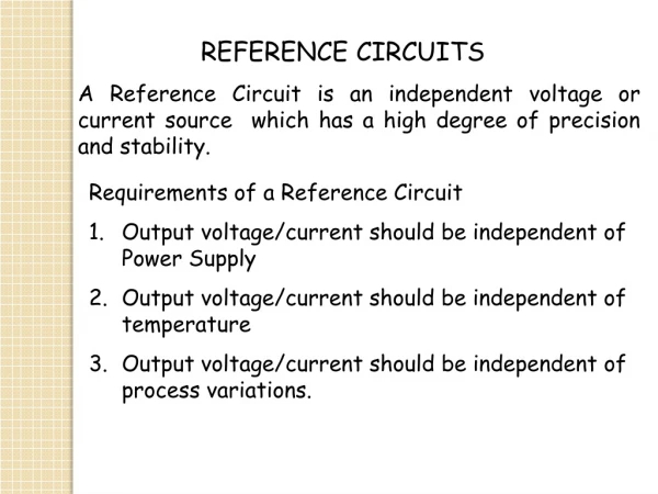
REFERENCE CIRCUITS
REFERENCE CIRCUITS. A reference circuit is an independent voltage or current source which has a high degree of precision and stability. Output voltage/current should be independent of power supply. Output voltage/current should be independent of temperature.

REFERENCE CIRCUITS
E N D
Presentation Transcript
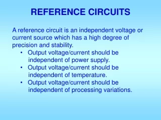
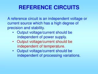
REFERENCE CIRCUITS • A reference circuit is an independent voltage or current source which has a high degree of precision and stability. • Output voltage/current should be independent of power supply. • Output voltage/current should be independent of temperature. • Output voltage/current should be independent of processing variations.
Types of commonly used references • Voltage dividers - passive and active. • MOS diode reference. • PN junction diode reference. • Gate-source threshold reference circuit. • Base-emitter reference circuit. • Thermo voltage reference circuit • Bandgap reference circuit
Typical variations affecting the references • Power supply variation (main concern here) • Load variation (ro=∞ for I-ref, ro=0 for V-ref) • Temperature variation (main concern also) • Processes variation (good process and layout) • Interferences and noise (not considered here)
VGS based Current reference MOS version: use VGS to generate a current and then use negative feed back stabilize i in MOS Start up Current mirror VGS
VEB based current reference Start up VEB=VR Negative temp coefficient
A cascoded version to increase ro and reduce sensitivity: Requires start up Not shown here VEB reference
A thermal voltage based current reference Current mirror I1 = I2, J1 = KJ2, but J = Jsexp(VEB/Vt) J1/J2 = K = exp((VEB1─ VEB2)/Vt) VEB1─ VEB2 = Vt ln(K) I = (VEB1─ VEB2)/R = Vt ln(K)/R Vt = kT/q J2 J1 PTAT
A band gap voltage reference Vout = VEB3 + I*L*R = VEB3 + (kT/q)*Lln(K) Vout/T = VEB3/T + (k/q)*Lln(K) At room temperature, VEB3/T = ─2.2 mV/oC, k/q = +0.085 mV/oC. Hence, choosing appropriate L and K can make Vout/T=0 When this happens, Vout = 1.26 V PTAT PTAT Negative temp coefficient
General principle of bandgap reference Generate a negatively PTAT (Proportional To Absolute Temperature) and a positively PTAT voltages and sum them appropriately.
VBEis negatively PTAT at roughly -2.2 mV/°C at room temperature, called CTAT Vt(Vt = kT/q) is PTAT that has a temperature coefficient of +0.085 mV/°C at room temperature. Multiply Vtby a constant K and sum it with the VBEto get VREF = VBE+ KVt If K is right, temperature coefficient can be zero.
VOSrepresents input offset voltage of the amplifier. Transistors Q1 and Q2 are assumed to have emitter-base areas of AE1 and AE2, respectively. If VOSis zero, then the voltage across R1 is given as
Converting a bandgap voltage reference to a current reference
Bandgap circuit formed by transistors M1, M2, M3, Q1, Q2, resistors R0, R2A, R2B, and R3. Cc is inter-stage compensation capacitor. Think of M2 as the second stage of your two stage amplifier, then Cc is connected between output B and the input Vc.
Amplifier: MA1~MA9, MA9 is the tail current source, MA1 and MA2 consistent of the differential input pair of the op amp, MA3~MA6 form the current mirrors in the amplifier, MA7 converts the amplifier output to single ended, and MA5 and MA8 form the push pull output node. • The offset voltage of the amplifier is critical factor, use large size differential input pair and careful layout; and use current mirror amplifier to reduce systematic offset. • 2V supple voltage is sufficient to make sure that all the transistors in the amplifier work in saturation. • PMOS input differential pair is used because the input common mode range (A,B nodes) is changing approximately from 0.8 to 0.6 V and in this case NMOS input pair won’t work. • Self Bias: MA10~MA13, a self-bias approach is used in this circuit to bias the amplifier. Bias voltage for the primary stage current source MA13 is provided by the output of the amplifier, i.e. there forms a self-feedback access from MA8 drain output to bias current source MA9 through current mirror MA10~MA13. • Startup Circuit: MS1~MS4. When the output of the amplifier is close to Vdd, the circuit will not work without the start-up circuit. With the start-up circuit MS1 and MS2 will conduct current into the BG circuit and the amplifier respectively.
Cc is 1 pF To have better mirror accuracy, M3 is driving a constant resistor Rtot. Capacitors at nodes A and B are added.
BG Circuit with simple bias circuit No self biasing No startup problem, no startup circuit needed Amplifier current depends on power supply voltage
Loop gain simulation Cc=0 F , Phase Margin = 37.86o
Phase Margin = 47.13o Cc=1pF
Cc+R compensation, 1pF+20kOhm Phase Margin = 74.36o
gA is the total conductance of node A, and gA = go1+gA’, gB is the total conductance of node B, and gB = go2+gB’, gZ is the total conductance of node Z CA, CB and CZ are the total capacitance at nodes A, B and Z
Then the open loop transfer function from Vi+/- to Vo+/- is The transfer function with CC in place is
a nulling resistor RC can be added in series with CC to push z1 to higher frequency
BG Circuit 3 with modified self-biasd circuit Reduce one transistor in the self-biased loop to change the type of the feedback
Cc=1 pF, Phase Margin = 56.99o Lower bandwidth
Characterization of a bandgap circuit Assuming an ideal op amp with an infinite gain, we have VA = VBand I1 = I2. Schematic of the current-mode bandgap circuit
For the silicon, α=7.021×10⁻⁴V/K, β=1108K, VG(0)=1.17V Since R1=R2, we know IC1 = IC2. Solving for Vbe2: Substituting back
We know I1=IC1+VA/R1. That gives Take partial derivative of I1 with respect to temperature For a given temperature, set the above to 0 and solve for R1. That tells you how to select R1 in terms of temperature, area ratio, and R0. Other quantities are device or process parameters.
In most literature, the last two items are ignored, that allows solution of inflection temperature T0 in terms of R0, R1, area ratio: The current at the inflection point is
Curvature and sensitivity The second-order partial derivative of I1 wrpt T is Notice that under a specific temperature, the second-order derivative is inversely proportional to the resistance R1. We would like to have small variation of I1 around TINF, so it is preferable to have a large R1.
The sensitivity of TINF wrpt R0 and R1 are For R1 = 13.74 KOhm and R0 = 1 KOhm, the sensitivity wrpt R0 is about -6.75, and about 6.5 wrpt R1, when A2/A1 is equal to 8.
Effects of mismatch errors and the finite op amp gain First, suppose current mirror mismatch leads to mismatch between Ic1 and Ic2. In particular, suppose: Re-solve for VA
Finally we get the first line is IC1 and the second is VA/R1 The derivative of I1 wrpt T becomes
Define similar to before: we can calculate
The sensitivity of TINF wrpt the current mismatch is This sensitivity is larger than those wrpt the resistances. That requires the current mismatch be controlled in an appropriate region so that the resistances can be used to effectively tune the temperature at the inflection point. The sensitivity of TINF wrpt the voltage difference is which means the inflection point temperature is not very sensitive to the voltage difference.