TDC Design Schemes for Hit Timing Relations and Buffer Utilization in FPGA Systems
60 likes | 203 Vues
This document outlines two designs of Time-to-Digital Converters (TDC) focusing on hit timing relations in RF systems. Scheme I details how hits are sampled continuously with 250 MHz sampling and the time resolution of 1 ns, where only the first hit in user-defined time bins (ranging from 2 ns to 128 ns) is recorded to optimize buffer space in FPGAs. Scheme II emphasizes the systematic filling of buffer units up to a maximum time range of 5 µs, also addressing data management for readout upon triggering, ensuring efficient FPGA usage and addressing possible discontinuities.

TDC Design Schemes for Hit Timing Relations and Buffer Utilization in FPGA Systems
E N D
Presentation Transcript
TDC Design Scheme Da-Shung Su Wen-Chen Chang 2011/02/19
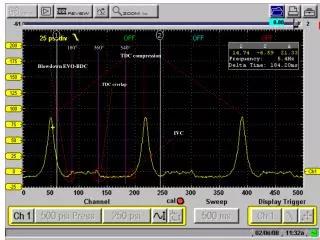
The Drift Time of Hits 20 ns RF Tmax.drift = 5 s
TDC Design Scheme I • After the issuing of “trigger enabled” (as an internal start), the input end will be continually sampled by 250 Mhz/4 Phases PLL with a counter. The 4 LSBs of the counter for a valid hit is written into a buffer region of FPGA. The time resolution of the LSB is 1 ns. If there is no hit happening, “0000” will be placed. • After the user-specified time bin (2, 4, 8, 16, 32, 64 or 128 ns), the point of writing is shifted to the next buffer unit. Only the first hit of supposed multiple hits within this time bin will be recorded.
TDC Design Scheme II • Such a sampling action will continue through all available buffer units and return to the every first after filling the last one. Considering that the maximum time range to be reached is “5 s” and the finest time bin “2 ns”, the number of available buffer units should be no less than 5000/2=2500 (Is it too many for FPGA?). • Upon receiving a trigger, data in the buffer units corresponding to “the matching window” (hopefully user-specified) is written into the FIFO to be readout. The time counter of the trigger is output as the data of channel 64. The discontinuity of TDC values across the reset of the time counter needs to be taken care.
FPGA Buffer for One Time Bin 32 bits