Download
1 / 5
50 likes | 211 Vues
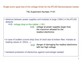
Single event upset test of the voltage limiter for the ATLAS Semiconductor tracker TSL Experiment Number: F151. distance between power supplies and modules is large (100m) in the ATLAS detector voltage drop on the cables (~3V)

E N D
Single event upset test of the voltage limiter for the ATLAS Semiconductor tracker TSL Experiment Number: F151 • distance between power supplies and modules is large (100m) in the ATLAS • detector • voltage drop on the cables (~3V) • voltage at power supplies larger than • the maximum allowed for the • readout electronics • in case of sudden current drop(loss of clock due to broken fiber, mistake at • loading values of DACs ...) • danger of damaging the readout electronics • with too high voltage • hardwareprotection of electronics against overvoltage needed
voltage limiter: • voltage at the shunt regulator (431) larger • than 2.5V opens the transistors q3 and q2 • which pass the current from Vdd(or Vcc) line • to the return lines. This current increases • voltage drop on cables and thus protects the • FE electronics. • voltage limit at the module is set by • the Rf and Re resistors • Vlim = 2.5V(1+Rf/Re) + 0.65V • limiters are there to guard the electronics • before power supplies react (few ms)
voltage limiters will be on PP3 inside experimental are UX15 • will be exposed to increased level of radiation which include • high energy particles • must be tested for radiation hardness • total dose tests have been done: 35krad and 6x10¹¹ n/cm2 (1MeV NIEL) • in the reactor in Ljubljana • must be tested for SEE with ~ 1011 p/cm2 ; Ep>60MeV • components that could be damaged by interaction of a high energy particle: • integrated circuit (TL431): bipolar IC can be very sensitive to latch-up • TEST: • voltage limiters will be exposed to the proton beam • performance will be periodically checked
scheme of the voltage limiter test system: • opening the switch ST1 causes current drop • measure maximal voltage on the module
4 limiter circuits must be irradiated • dimension of a limiter PCB ~ 2x4 cm2 (areaof sensitive part little smaller) • could irradiate all at once (arrange them in 5x5 cm2 area or put them one • behind another?) • limiters must be biased during irradiation (connection cables needed) • 1 table in the lab (outside of the beam area) needed for the power supplies and • readout equipment • total fluence (1011 p/cm2) should not be reached faster than in ~ 1h in order • to perform several measurements during irradiation