Breaking the Bandwidth Bottleneck in Telecommunications & Information Processing: New Electro-Optic Materials
510 likes | 742 Vues
10 th Foresight Conference on Nanotechnology October 11-13, 2002. Breaking the Bandwidth Bottleneck in Telecommunications & Information Processing: New Electro-Optic Materials. Larry Dalton Departments of Chemistry, Materials Science & Engineering, and Electrical Engineering

Breaking the Bandwidth Bottleneck in Telecommunications & Information Processing: New Electro-Optic Materials
E N D
Presentation Transcript
10th Foresight Conference on Nanotechnology October 11-13, 2002 Breaking the Bandwidth Bottleneck in Telecommunications & Information Processing: New Electro-Optic Materials Larry Dalton Departments of Chemistry, Materials Science & Engineering, and Electrical Engineering University of Washington & University of Southern California Acknowledgements Financial support provided by the National Science Foundation and the Air Force Office of Scientific Research
Critical to Next Generation Computing •Semiconductor Research Corporation Workshop on Optical Interconnects http://www.src.org/member/sa/nis/E002117_Opto_wksp.asp •British House of Lords Select Committee on Science & Technology Study of Innovations in Computer Processors •Forthcoming article in IEEE Computing •High frequency, ultra high stability clocks •On-chip signal distribution •Chip-to-chip interconnection •Module-to-module interconnection
Critical to Telecommunications Industry From: "PARK,CHRIS (A-England,ex1)" <chris_park@agilent.com> To: "'Larry Dalton'" <dalton@chem.washington.edu> Cc: "MEADOWCROFT,SIMON (A-England,ex1)" <simon_meadowcroft@agilent.com> Subject: Collaboration with Agilent Technologies Date: Tue, 2 Jan 2001 15:54:07 +0100 Dear Prof Dalton, Agilent Technologies would like to meet with you to find out more about your work on high speed polymer modulators. Our interest is based on a need to manufacture low cost 100 Gigabit Ethernet optical components in approximately 3 years time using technologies which are compatible with high volume and low manufacturing cost. The work you have published on high speed modulators is currently one of the best alternatives for a low component count, low modulation voltage 100GbE transmitter. Agilent Technologies would therefore be interested in discussing your work and the options for collaboration. These options can include research sponsorship and/or business development including support for new start-up activity. Simon and I will be attending OFC in Anaheim and would like to meet with you that week, or if you are not attending OFC we could visit Washington early the following week (w/c 26th March).Please let us know whether you are available at this time. Best regards Dr Chris Park Research ManagerAgilent Technologies Whitehouse Rd, Ipswich, UK Tel 44 1473 465628 e-mail chris_park@agilent.com
Electro-Optic Devices: The on-ramps & interchanges of the information superhighway(The Metro Loop and Fiber to the Home)
Critical to Defense Industry Caltech U Washington
Electro-Optics: The Phenomena • An electro-optic material (device) permits electrical and optical signals to “talk” to each other through an “easily perturbed” electron distribution in the material.A low frequency (DC to 200 GHz) electric field (e.g., a television [analog] or computer [digital] signal) is used to perturb the electron distribution (e.g., p-electrons of an organic chromophore) and that perturbation alters the speed of light passing through the material as the electric field component of light interacts with the perturbed charge distribution. • Because the speed of light is altered by the application of a control voltage, electro-optic materials can be described as materials with a voltage-controlled index of refraction. Index of refraction = speed of light in vacuum/speed of light in material
Electro-Optic Devices: The on-ramps & interchanges of the information superhighway • The electro-optic effect can be used to transduce electrical information (signals) onto the internet (in to optical signals). By slowing light down in one arm of the Mach Zehnder device shown below, the interference of light beams at the output can be controlled. Electrical information appears as an amplitude modulation on the optical transmission. This works equally well for analog or digital data. Modulated Light Out Light In
What are the critical requirements for EO materials and devices? • Low halfwave voltage is a critical requirement in externally modulated photonic systems: • Analog systems: For RF transparency: • Link gain 1/Vp2 • For high dynamic range: • NF Vp2 • (low level signal detection limited by noise floor) • Digital systems: • High speed digital circuits have low output voltage • Digital amplifiers very costly • Bandwidth is the other critical requirement!
Why Organic Electro-Optic Materials (Devices)? •Intrinsic material bandwidths of several hundred gigahertz. The response time (phase relaxation time) of p-electrons in organic materials to electric field perturbation is on the order of femtoseconds. Operational bandwidths of 150 GHz have been demonstrated for modulators & switches •Organic electro-optic coefficients are currently 2-4 times higher than lithium niobate and getting larger. Theoretically-inspired rational design of materials will keep electro-optic activity improving for several years. Device operational voltages of less than 1 volt are routine. •Organic EO materials are highly processable into 3-D circuits and can be easily integrated with semiconductor VLSI electronics and silica fiber optics. Low loss coupling structures can be straightforwardly fabricated. .
Comparison of Lithium Niobate and Polymer Electro-Optic Modulators State-of-the-art High Speed Infrared Modulators Commercial Lithium Niobate Devices—The Competition Vp: 6 V @1550 nm, 30 GHz Bandwidth, $6000/per unit Commercially Available Polymer Devices Vp: 1.2 V @ 1300 nm, 1.8 V @1550 nm 20 GHz and 30 GHz Bandwidth (3dBe) Published Prototype Device Results Vp: 0.77 V @ 1300 nm 100 GHz operation Recent Dendrimer Device Results Vp: 0.5 V @ 1550 nm Recent MR Device Results Vp: < 1 V @ 1550 nm 10 Modulator Chips on 3 Inch Wafer 2 Push-Pull MZ Modulators on One Chip
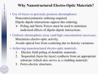
Why Nanostructured Electro-Optic Materials? •Noncentrosymmetric ordering of chromophores (all pointing in the same direction) in the material lattice is required for electro-optic activity. Chromophore dipole-dipole interactions oppose this ordering. Forces must be used to achieve the desired order and chromophores must be positioned precisely in space to minimize the undesired effects of dipole-dipole interactions. •A uniform chromophore distribution (and high concentration) is necessary not only to maximize electro-optic activity but also to avoid optical loss from scattering off of material density (index of refraction) variations. •Several routes to nanostructured electro-optic materials are being pursued including (1) the electric field poling of dendritic materials and (2) sequential (layer-by-layer) synthesis from an appropriate substrate (which also serves as a cladding material).
Theoretically inspired rational improvement of organic electro-optic materials •Theory (quantum and statistical mechanics have guided the systematic improvement of the hyperpolarizability (b) of organic chromophores and the electro-optic activity of macroscopic materials, e.g.,
Systematic Improvement in Molecular Electro-Optic Activity: Variation of mb
New Advances in Chromophore Development Quantum mechanical calculations permit the optimization of the p- electron structure that defines molecular hyperpolarizability. New Synthesis Techniques: Microwave synthesis techniques permit dramatic enhancement in reaction yields and synthesis of new materials. . New Paradigm: Gradient- Bridge, Mixed- Ligand-Acceptor Chromophores
Why Microwave Synthesis? •Microwave synthesis has permitted dramatic enhancement in reaction yields, reducing time devoted to purification. It has also permitted many materials to be synthesized for the first time and has permitted greater flexibility in reaction conditions. •Microwave synthesis techniques obviously permit more uniform heating of reaction mixtures. The absence of thermal gradients and “hot spots” helps minimize decomposition and side reactions. Microwave synthesis permits the use of a wider range of solvents. •We have found this approach to be particularly effective for condensation, addition, and de-protection reactions. .
Comparison of Microwave & Reflux Synthesis of CF3-TCF acceptor
Microwave Synthesis: Examples of Syntheses of New Acceptors .
Translating Microscopic to Macroscopic Electro-Optic Activity
Comparison of Potential Functions from Analytic Theory & Monte Carlo Calculations Points—Monte Carlo Calculation Solid Line—Analytic Theory Centric Order . Acentric Order
Comparison of Theory & Experiment Experiment—Solid Diamonds .
Theory-Guided Nano-Engineering: Generalization of the Use of Dendronized Chromophores New Paradigm: The Concept of Dendronized Chromophores Can Be Generalized. .
Statistical Mechanics Guides the Optimization of Macroscopic Electro-Optic Activity New Paradigm: Dendrimer synthesis of theoretically-predicted optimum chromophore shapes—nano-architectural engineering. . With electric field poling and crosslinking, multi-chromophore dendrimers assume partially closed umbrella-like shapes. Also, these dendrimers don’t interpenetrate. These two observations are supported by theoretical calculations and experimental observations.
Control of Intermolecular Electrostatic Interactions Using Multi-Chromophore Dendrimers Twice the EO activity of same chromophore in polymer matrix—record value at 1.55 microns. Factor of 2 in thermal stability. Thermal stability of EO activity at 85 C Jen, Dalton et al., J. Am. Chem Soc, 123, 986 (2001)
Dendronized Chromophores: An example Dendronized chromophore yields 3 times the electro-optic activity and reduced optical loss (next figure). .
Perfluorodendron-substituted Chromophore Contributes Little to Optical Loss in Guest-Host APC Polymer 0.85 dB/cm at 1.55 mm 0.68 dB/cm at 1.3 mm
Perfluroinated Chemophore-Containing Dendrimers: Low Total Optical (Absorption and Scattering) Loss
THERMAL STABILITY—The Need to Lock-In Poling Induced Acentric Order: Intermolecular Crosslinking
Optimizing Photostability •Photochemical stability can be improved by chromophore design. Lumera has demonstrated this. •Photochemical stability can be improved by the use of scavengers (see below), packaging, and lattice hardening. .
Improvement in Photostability by Simple Packaging Photostability--Packaged in Argon • 50 mW (1550nm) at the output fiber • Exposed over 30 days, Vp change negligible • Reduce free O2 . Clearly some oxygen is present in this test.
Processability: An Advantage of Organic Electro-Optic Materials •The tailorability of organic materials and particularly of dendrimers permits integration of organic EO materials with virtually any material (silicon, silicon dioxide, Mylar, III-V semiconductors, metals, etc.) •Hardened organic EO materials are amenable to reactive ion etching (RIE) and to various photolithographic processes. Processing is very compatible with semiconductor processing techniques. •Organic materials are quite robust (high dielectric breakdown, good thermal stability at most processing temperatures, high radiation (gamma, high energy particle) damage thresholds, etc. •Likely amenable to high volume manufacturing using processing techniques such as spin casting and dry etching. •Straightforward fabrication of an array of prototype devices.
Fabrication of Vertical Slope Using Gray Scale Mask Lithography
Fabrication: Shadow Etch Oxygen Ions • Shadow Masking of Ions • Angle µ RF Power, Gas Pressure, Time, Mask Dimensions • Angles: 0.1-3° • Heights: 1-9mm • Lengths: 200-2,000mm • Fast Prototyping • Various Angles From Single Mask • No Extensive Fabrication Steps • Repeatable Quality Mask Offset Polymer 6 4 m Height (m) 2 0 0 400 800 1200 1600 Length (mm)
Tapered Transitions: Minimization of Coupling Loss n(active) > n(passive) small length Þ material loss ß large length Þ radiation loss ß
Fabrication Lower Electrode Vertical Slope Upper Coatings Waveguide Ridge
Integrated wavelength add-drop filter Re-configurable optical waveguide cross connect. The streets and avenues are fabricated on different levels with the ring resonator switches in between at each junction. Modulates l3 Modulates l1 Modulates l2 WDM modulation module. Each wavelength modulated by separate resonate modulator. Laser l1, l2, l3 IMPROVED PROCESSABILITY: POLYMER MICRO-PHOTONIC RING RESONATORS l2 l1 l3 l1, l2, l3
Au upper modulation electrode Complementary modulated output Modulated output Input Au Au UFC 170 3mm SU-8 4.5mm CLD1 CLD1 5mm UV15 Au Si CROSSECTION GND POLYMER MICRO-PHOTONIC RING RESONATOR USING ELECTRO-OPTIC POLYMERS • Why Polymers? • Wide range of indices of refraction • Easy fabrication on multiple levels and integration with other devices • Voltage tunable filter or switch/ modulator using electro-optic polymers • Compact structure; size limited by index contrast • Temperature tuning, 0.1nm/C (use as an advantage or eliminate by athermal design • in which thermal expansion of polymer substrate balances dn/dT of waveguide)
Gold ground GND Au Electrode SU-8 INTEGRATED WDM TRANSMITTER-RECIEVER Eye diagram 1 Gb/s, Vpeak = 1 V Device has ~2GHz BW = 2 GHz/V
Large Angle, Fast Response Spatial Light Modulator (SLM) Experimental Results Schematic Diagram Literature Citations • Dalton, Steier, et al., “Polymeric waveguide prism based electro-optic beam deflector,” Opt. Eng., 40, 1217-22 (2001) • Dalton, Steier, et al., “Beam deflection with electro-optic polymer waveguide prism array,” Proc. SPIE, 3950, 108-116 (2000) • Dalton, Steier, et al., “Polymeric waveguide beam deflector for electro-optic switching,” Proc. SPIE, 4279, 37-44 (2001) Photonic Band Gap Fabrication
Phased Array Radar with Photonic Phase Shifter (1 of 3 approaches) Dalton, Steier, Fetterman, et al., IEEE mW & Guided Wave Lett., 9, 357 (1999)
High Bandwidth, Ultrastable Oscillators (Signal Generators) • Dalton, Steier, Fetterman, et al., “Photonic control of terahertz systems,” Terahertz Electronic Proceedings, 102-5 (1998) • Dalton, Steier, Fetterman, et al., “Electro-optic applications,” in Encyclopedia of Polymer Science and Technology (J. Kroschwitz, ed) Wiley & Sons, NY, 2001
100 Gbit/sec Analog-to-Digital Converter(1 of 2 approaches) • Dalton, Steier, Fetterman, et al. “Time stretching of 102 GHz millimeter waves using a novel 1.55 mm polymer electrooptic modulator,” IEEE Photonics Technology Letters, 12, 537 (2000)) • Dalton, Steier, Fetterman, et al. “Photonic time-stretching of 102 GHz millimeter waves using 1.55 mm polymer electro-optic modulator,” Proc SPIE, 4114, 44 (2000).
High Bandwidth Optical Modulators and Switches (The Electrical Problem) Two bands approach: • DC-65 GHz direct modulation, use one modulator section; • 65-130 GHz using upconversion scheme, RF applied to one modulator section, and LO applied to the other section. Steier, Bechtel, Dalton et al., Proc. SPIE, 4114, 58-64 (2000).