Plasmon Induced Electrical Conduction in Molecular Devices
50 likes | 242 Vues
Plasmon Induced Electrical Conduction in Molecular Devices. Parag Banerjee,† David Conklin,‡ Sanjini Nanayakkara,‡ Tae-Hong Park,§ Michael J. Therien, and Dawn A. Bonnell‡,* ACS Nano on line Jan 2010. Plasmon Induced Electrical Conduction in Molecular Devices

Plasmon Induced Electrical Conduction in Molecular Devices
E N D
Presentation Transcript
Plasmon Induced Electrical Conduction in Molecular Devices Parag Banerjee,† David Conklin,‡ Sanjini Nanayakkara,‡ Tae-Hong Park,§ Michael J. Therien,and Dawn A. Bonnell‡,* ACS Nano on line Jan 2010
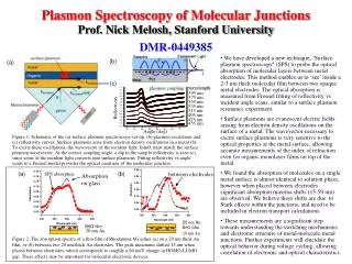
Plasmon Induced Electrical Conduction in Molecular Devices Parag Banerjee, David Conklin, Sanjini Nanayakkara, Tae-Hong Park, Michael J. Therien,and Dawn A. Bonnell Plasmonics is a new field in which surface plasmons are exploited to manipulate and control light. Here we show that surface plasmons can be configured to induce electronic transport in molecular devices and in this manner convert optical energy into electrical conduction. Hybrid nanostructures were fabricated in which 32 nm gold particles are linked with optically active porphyrin molecules. The structures are designed such that the spacing between many of the particles is exactly the length that the molecules span. The plasmons focus light to the junction and induce electrical conduction by localizing photon flux to increase exciton production in the molecule. The transport properties of the molecule, the proximity of the gold electrodes and the plasmons lead to current enhancements by factors of 4-20 (400% to 2000%) even in these unoptimized devices. These results suggest new strategies for energy efficient circuits, energy harvesting coatings, optical circuit components, and neural logic devices. Banerjee, et al ACS Nano 2010
The plasmon mediated molecular device is a tiny (invisible) object that spans a small part of the light contrast line within the circle on the chip. 1000 junctions span that line.