Download
1 / 4
40 likes | 241 Vues
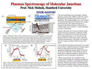
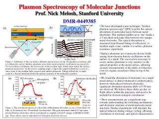
595 nm. 575 nm. 555 nm. 535 nm. 515 nm. 495 nm. 475 nm. 455 nm. between electrodes. Plasmon Spectroscopy of Molecular Junctions. Prof. Nick Melosh, Stanford University. DMR-0449385.

E N D
595 nm 575 nm 555 nm 535 nm 515 nm 495 nm 475 nm 455 nm between electrodes Plasmon Spectroscopy of Molecular Junctions Prof. Nick Melosh, Stanford University DMR-0449385 • We have developed a new technique, ‘Surface plasmon spectroscopy’ (SPS) to probe the optical absorption of molecular layers between metal electrodes. This method enables us to ‘see’ inside a 2-3 nm thick molecular film between two opaque metal electrodes. The optical absorption is measured from Fresnel fitting of reflectivity vs incident angle scans, similar to a surface plasmon resonance experiment. • Surface plasmons are evanescent electric fields arising from electron density oscillations on the surface of a metal. The wavevector necessary to excite surface plasmons is very sensitive to the optical properties at the metal surface, allowing accurate measurements of the index of refraction even for organic monolayer films on top of the metal. • We found the absorption of molecules on a single metal surface is almost identical to solution phase, however when placed between electrodes significant absorption maxima shifts (15-50 nm) are observed. We believe these shifts are due to Stark effects within the junctions, and need to be included in electron transport calculations. • These measurements are a significant step towards understanding the switching mechanisms and electronic structure of metal-molecule-metal junctions. Further experiments will elucidate the optical behavior during voltage cycling, allowing correlation of electronic and optical characteristics. (b) (a) (c) wavelength plasmon coupling Reflectivity Angle (deg) Figure 1: Schematic of the (a) surface plasmon spectroscopy set-up, (b) plasmon excitations and (c) reflectivity curves. Surface plasmons arise from electron density oscillations in a metal (b). To excite these oscillations, the wavevector of the incident light, ksinq, must match the surface plasmon wavevector. At the correct coupling angle, a dip in the sample reflectivity is seen (c), since some of the incident light converts into surface plasmons. Fitting reflectivity vs angle scans to a Fresnel model provides the optical constants of the molecular junction. (a) (b) SPS absorption Absorption on glass 20 nm Au R6G film R6G film 20 nm Au 20 nm Au Figure 2: The absorption spectra of a thin film of Rhodamine 6G either (a) on a 20 nm thick Au film, or (b) between two 20 nm-thick Au electrodes. The peak maximum shifted 15 nm when placed between electrodes, which corresponds to roughly a 60 meV change in HOMO-LUMO gap. These effects may be important for molecular electronic devices.
PA-LOFO carboxylic acid monolayer evaporated electrode suspended electrodes crossbar device Polymer lift-on lift-off Aluminum Au film 1mm Substrate water bottom electrodes H3C-(CH2)n-COOH b = 0.85 Å-1 Lift-on gold electrode 6 electrodes on a 1” cover slide Polymer Assisted Lift-Off Float-On Electrodes (PA-LOFO) (1) (2) (3) (4) (5) • We developed a new way to softly deposit the top metal contacts onto an organic film. Depositing the top metal contact for molecular electronics is always difficult, especially to achieve near-atomically flat films. Sputter or e-beam deposited metals always damage the organic sample to some extent, while other ‘soft’ methods like lift-off float-on electrodes wrinkled excessively and stamped contacts were always very rough. • We used a thin polymer as a backing to support evaporated metal electrodes, which gave them mechanical strength and hydrophobicity. • These contacts had the same optical and electrical properties as directly evaporated metal on a smooth substrate, thus the PA-LOFO procedure did not appear to harm the metal in any way, such as cracking or buckling. • Electrode arrays with wire widths as small as 1 micron to as large as 3 mm and up to 3 cm in length could be fabricated without wrinkling. • Studies of electron tunneling through carboxy alkanes with a PA-LOFO top contact show the same tunneling behavior as literature STM and nanopore measurements. Even with 4 mm2 contact areas, no shorting is observed. Figure 3: Sequence to deposit top metal contacts using the PA-LOFO technique. (1) Patterned metal electrodes (as thin as 10 nm) are deposited onto a Si or mica substrate and coated with a polymer backing layer. This film is dipped into a dilute KOH solution to weaken the polymer-substrate adhesion. (2) the sample is transferred into a water bath, where the polymer and metal peel away from the substrate. (3) The hydrophobic polymer causes the electrodes to float on top of the water. (4) The bottom electrodes with the molecular film is dipped beneath the floating polymer/metal film, and lifted into contact with the floating electrodes. (5) UV/ozone or O2 plasma can be used to remove the polymer layer, leaving the completed molecular crossbar device. (a) (a) (b) (b) Figure 5: (a) Schematic of a metal-molecule-metal junction with a Langmuir-Blodgett fatty acid films and a PA-LOFO top electrode. (b) Tunneling current though the molecular monolayer. A fit to a Simmons tunneling model gives the decay constant b= 0.85 Å-1, similar to literature reports, indicating no shorting and good metal electrodes. Figure 4: (a) Float-on electrode transferred onto a glass substrate from a water bath. Each electrode is 2 mm wide and 2 cm long. (b) Optical microscope image of an evaporated Al bottom electrode with a fatty acid LB film with a 20 nm thick PA-LOFO Au electrode deposited on top. Note the lack or wrinkles or asperities of the Au.
(a) Absorbance (a.u.) (b) Absorbance (a.u.) wavelength (nm) Molecular Electronics: Rotaxane Switching One of the most controversial molecular electronic systems is the conductance switching behavior of [2]-rotaxanes within a molecular junction. Solution-phase studies have shown that the cyclophane ring encircling the rotaxane may be shuttled back and forth between two electron rich moieties along the dumbbell-like core, however whether this behavior persists when the molecules are placed between metal electrodes is unknown. In particular, the question is whether or not changes in the position of the molecular cyclophane ring are correlated with the conductance switching observed in the remnant current-voltage scans. • Rotaxanes exhibit two different absorption spectra in solution depending on where the cyclophane ring is located. When the ring is on the napthalene group, the rotaxane is a red color, while on the tetrathiafulvalene (TTF) group it is green. In solution, this particular rotaxane was a mixture both red and green conformations. • Using our surface plasmon spectroscopy (SPS) technique, we have been able for the first time to directly measure the absorption spectrum of a rotaxane monolayer between two metal electrodes (Figure 6b). We find that just as in solution, the rotaxane monolayer between electrodes has a distribution between both red and green conformations. • We have been able to reproduce the rotaxane monolayer conductance switching others have reported using our PA-LOFO technique to create large area electrodes (4 mm2) without electrical shorting. The remnant current switching behavior was reproducible and could be cycled over 10 times (figure 7) • Upcoming research will determine whether the “high” and “low” conductance state correlate to a particular location of the cyclophane ring as determined by SPS. napthalene TTF group cyclophane ring Remnant Current Measurements “high” state “low” state Figure 6. (a) UV-vis absorption spectra of [2]-rotaxane molecules in CHCl3 solution with the cyclophane ring either on the TTF group (green line), or the napthalene group (red line). Adapted from Ballardini et al, New J. Chem. 2001 (b) Surface plasmon spectrum of Al-Au junction (white) and Al- rotaxane-Au junction (green). This rotaxane exhibited mixed conformations (red and green from (a)) in solution, which is also observed in the solid state device. Figure 7. Remnant current measurement of a [2]-rotaxane Langmuir Blodgett monolayer between Al and Au electrodes. We observed voltage-induced switching very similar to that of Luo, ChemPhysChem, 2002. The red trace is the remnant current measured at a constant voltage of 100 mV, and the black trace is the applied ‘write’ voltage. Repeated cycling (b) shows an initial decay in remnant current, after which the switching magnitude stabilizes.
Teaching Others about Science Over the past year, the Melosh group has hosted three undergraduates (Adam Freund, Jim Jelincic, and Vimalier Reyes-Ortiz) and one high school student (Dan Vinson, from Palo Alto High) to order to give younger students access to the excitement of real hands-on research. One student, Vimalier, came from Puerto Rico for the summer to see what working in a large laboratory was like. After the summer research, he defended his work in a public presentation, and has since decided to go to graduate school and to seek a position in the high-tech industry. In addition, in June 2005 Dr. Melosh visited Homestead High, a local under-privileged high school, on several occasionsin an NSF-supported effort to invigorate young people with an interest in science. In co-ordination with local science teacher Jillian Fackrell, these visits sought not just to excite students about our work and materials science, but encourage an interest in a scientific career by presenting work and anecdotes from a wide variety of researchers. Students got to test the modulus of crystalline metals vs metallic glasses, demonstrate the principle of ‘sacrificial bonds’ within living systems, and discover the amazing phenomena of shape-memory alloys. These visual and hands-on demonstrations gave students a concrete idea of what types of exciting careers might spring from a degree in science. At the end of the school year, more than a quarter of the students mentioned that they had really liked the opportunity to see ‘real science’ first hand. Future visits over the coming year will feature demonstrations integrated into their curriculum throughout the school year, and a chance to intern in our labs over the summer.