I. ELECTRICAL CONDUCTION
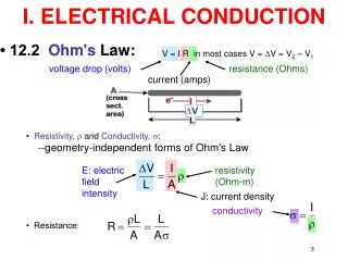
I. ELECTRICAL CONDUCTION. • 12.2 Ohm's Law:. V = I R in most cases V = D V = V 2 – V 1. voltage drop (volts). resistance (Ohms). current (amps). • Resistivity, r and Conductivity, s : --geometry-independent forms of Ohm's Law. E: electric field intensity. resistivity

I. ELECTRICAL CONDUCTION
E N D
Presentation Transcript
I. ELECTRICAL CONDUCTION • 12.2 Ohm's Law: V = I R in most cases V = DV = V2 – V1 voltage drop (volts) resistance (Ohms) current (amps) • Resistivity, r and Conductivity, s: --geometry-independent forms of Ohm's Law E: electric field intensity resistivity (Ohm-m) J: current density conductivity • Resistance: 3
c12f01 c12f01
c12f02 c12f02
c12f03 c12f03
c12f04 c12f04
12.6 Conduction in Terms of Band and Atomic Bonding Models Metallic character Excitation barrier is much smaller than heat (RT), noise or any background excitations. Practically anything excite electrons to the conduction band c12f05
An intrinsic semiconductor has a band gap or barrier for the electrons to get into the conduction band This barrier need a photon excitation, an external bias potential Usually RT cannot excite the electron to the conduction band. For instance, a photon of light ~4eV c12f06 c12f06
12.7 Electron Mobility c12f07 Scattering Events Electric field drifts electrons in the opposite direction to the field b/c electrons are –ve The actual speed of electrons is much higher than the drift velocity Scattering is due to the strike with the nuclei When the actual velocity of the electrons is similar to the drift velocity, the system is in the ballistic regime In the ballistic regime there is practically no barrier for the electrons Examples: in vacuum tubes, ~in carbon nanotubes (CNT), superconductors* J = sE c12f07
II. SEMICONDUCTIVITY Conductivity of semiconducting materials is lower than from metals Sensitive to minute concentrations of impurities Intrinsic: pure material Extrinsic: doped with impurity atoms 12.10 Intrinsic Semiconduction Band structure Si (1.1 eV) Ge (0.7 eV) GaAs (IIIA-VA) InSb (IIIA-VA) CdS (IIB-VIA) ZnTe (IIB-VIA) We have electrons as carriers in metals and “electrons” and ‘holes’ as carriers in semiconductors
c12f13 n-type extrinsic semiconductor c12f13
c12f14 p-type extrinsic semiconductor c12f14
c12f15 p-type extrinsic semiconductor c12f15
Intrinsic carrier increases rapidly with temperature c12f16 c12f16
c12f17 n-type silicon 1021/m3 c12f17
12.14 The Hall Effect c12f20 How we can determine the type of carriers? Use magnetic fields The Hall voltage The Hall coefficient c12f20
p-n rectifying junction c12f21 Flow of electrons in one direction only convert alternating current to direct current Processing: diffuse P into one side of a B-doped crystal. • Results: --No applied potential, no net current flow. --Forward bias: carriers flow through p-type and n-type regions; holes and electrons recombine at p-n junction; current flows. --Reverse bias: carrier flow away from p-n junction; carrier conc. greatly reduced at junction; little current flow. c12f21
c12f22 c12f22
c12f23 c12f23
The Junction Transistor c12f24 c12f24
The Junction Transistor c12f25 c12f25
c12f26 The MOSFET c12f26
12.17 Electrical properties of polymers c12eqf01 Usually poor conductors of electricity Mechanism not well-understood Conduction in polymers of high purity is electronic Conducting Polymers Conductivities of 1.5x10⁷ (W-m)-1 Even polyacetylene Due to alternating single-double bonds
Dielectric material Electric dipole structure Charge separation Do = eoE c12f28 eo= permittivity of vacuum = 8.85x10⁻¹² F/m Do = eoE + P Dielectric Behavior
c12tf05 c12tf05
12.19 Field vectors and polarization c12f29 p = qd Surface charge density or dielectric displacement (C/m2) Do = eoE For the dielectric case D= e E
c12f31 Do = eoE + P where P is the polarization (C/m2) or total dipole moment per unit of volume of the dielectric P= eo(er– 1)E
c12f32 Electronic Polarization c12f32 Ionic polarization Orientation polarization
12.21 Frequency Dependence of the dielectric constant c12f33 Response to alternating fields Reorientation time --- relaxation frequency
c12f34 Frequency dependence of the dielectric constant c12f34
SUMMARY • Electrical conductivity and resistivity are: --material parameters. --geometry independent but not at small scale (nano) • Electrical resistance is: --a geometry and material dependent parameter. • Conductors, semiconductors, and insulators... --different in whether there are accessible energy states for conductance electrons. • For metals, conductivity is increased by --reducing deformation --reducing imperfections --decreasing temperature. • For pure semiconductors, conductivity is increased by --increasing temperature --doping (e.g., adding B to Si (p-type) or P to Si (n-type). 15

