Download
1 / 58
590 likes | 928 Vues
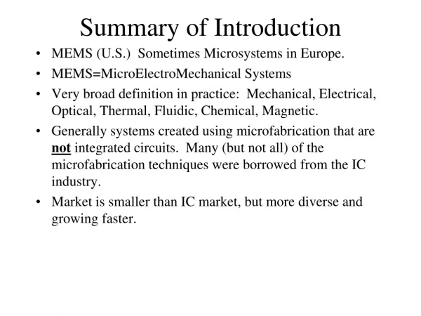
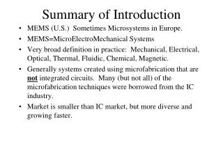
Summary of Introduction. MEMS (U.S.) Sometimes Microsystems in Europe. MEMS=MicroElectroMechanical Systems Very broad definition in practice: Mechanical, Electrical, Optical, Thermal, Fluidic, Chemical, Magnetic.

E N D
Summary of Introduction MEMS (U.S.) Sometimes Microsystems in Europe. MEMS=MicroElectroMechanical Systems Very broad definition in practice: Mechanical, Electrical, Optical, Thermal, Fluidic, Chemical, Magnetic. Generally systems created using microfabrication that are not integrated circuits. Many (but not all) of the microfabrication techniques were borrowed from the IC industry. Market is smaller than IC market, but more diverse and growing faster.
Some Examples • Accelerometer • Electrical/Mechanical • mTAS or Micro Total Analysis System • Purifies, amplifies, and detects DNA, for example. • Fluids/Biochemistry/Optical/Electrical • TI DLP • Optical/Mechanical/Electrical/Surface Science • Microrelay • Mechanical/Electrical/Surface Science • Microplasma Source • Electrical/Electromagnetic/Plasma • What do you need to know for MEMS? • Everything???!!! • Truly an interdisciplinary field.
What are we going to do? • Learn a useful subset of techniques needed for designing MEMS devices. Not all!! • We will design MEMS devices. • Project teaming survey is due Friday – see web site. • Project assignment is on the web site. • We will discuss examples of MEMS devics and use the techniques we have developed. • First we will look at microfabrication and process integration. • Other notes: • First homework is due today. (Some flexibility here – students joining class, thurn-in mechanism …) • Second homework is due on Tuesday.
Microfabrication: Types of Micromachining for MEMS • Bulk Micromachining • Etch away large parts of the silicon wafer. • Traditionally, KOH or other chemical etch. • Recently DRIE (Deep Reactive Ion Etch), an anisotropic plasma etch. • Surface micromachining • On surface of wafer/substrate • Sometimes can be a post-process on top of CMOS wafer for process integration with electronics. • Typically much thinner structures than bulk micromachining, but metal structures can be fairly thick. • LIGA • X-ray lithographie, galvanoformung, abformtechnik (or lithography, electrodeposition, and molding). • A special type of surface micromachining, not much used in its original form. • Now sometimes refers to using very thick photoresist to make thick electroplated structures.
Packaging Ideally, part of fabrication process, then just use a cheap plastic package. Often, a surface micromachined device is bonded to a bulk micromachined package (the cavity to contain the device is etched from the wafer using bulk micromachining). Sometimes the package is the most expensive part of the device (pressure sensors, microfluidics). Especially true when the device interacts with the outside environment.
References: Text (brief), Campbell or other IC fabrication text (generally good, but incomplete for MEMS), Madou (specific to MEMS).
Silicon wafer fabrication Taken from www.egg.or.jp/MSIL/english/index-e.html
Silicon wafer fabrication – slicing and polishing Taken from www.egg.or.jp/MSIL/english/index-e.html
LPCVD Systems Taken from http://www-bsac.EECS.Berkeley.EDU/~pister/245/
Gate Beam Drain Beam Source Drain Gate Source Gate Drain Source Electrodeposition/Electroplating Surface Micromachined Post-Process Integration with CMOS 20-100 V Electrostatic Actuation ~100 Micron Size SEM of NEU microswitch
Packaging Ideally, part of fabrication process, then just use a cheap plastic package. Often, a surface micromachined device is bonded to a bulk micromachined package (the cavity to contain the device is etched from the wafer using bulk micromachining). Sometimes the package is the most expensive part of the device (pressure sensors, microfluidics). Especially true when the device interacts with the outside environment.
Micromachining Ink Jet Nozzles Microtechnology group, TU Berlin
Bulk micromachined cavities Taken from http://www-bsac.EECS.Berkeley.EDU/~pister/245/ Anisotropic KOH etch (Upperleft) Isotropic plasma etch (upper right) Isotropic BrF3 etch with compressive oxide still showing (lower right)
Deposit sacrificial layer Pattern contacts Deposit/pattern structural layer Etch sacrificial layer Surface Micromachining Taken from http://www-bsac.EECS.Berkeley.EDU/~pister/245/
Residual stress gradients Taken from http://www-bsac.EECS.Berkeley.EDU/~pister/245/ More tensile on top More compressive on top Just right! The bottom line: anneal poly between oxides with similar phosphorous content. ~1000C for ~60 seconds is enough.
Residual stress gradients Taken from http://www-bsac.EECS.Berkeley.EDU/~pister/245/ A bad day at MCNC (1996).
DRIE structures Taken from http://www-bsac.EECS.Berkeley.EDU/~pister/245/ • Increased capacitance for actuation and sensing • Low-stress structures • single-crystal Si only structural material • Highly stiff in vertical direction • isolation of motion to wafer plane • flat, robust structures Thermal Actuator Comb-drive Actuator 2DoF Electrostatic actuator