Download
1 / 41
410 likes | 436 Vues
Explore the key components and diagrams of memory units including ROM, RAM, PLDs, and CPLDs. Learn about memory cycle timing, address multiplexing, and logic configurations.

E N D
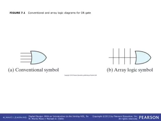
FIGURE 7.1 Conventional and array logic diagrams for OR gate
FIGURE 7.7 Two‐dimensional decoding structure for a 1K‐word memory
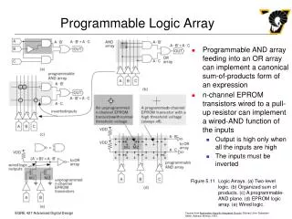
FIGURE 7.14 PLA with three inputs, four product terms, and two outputs
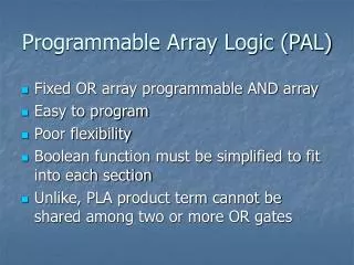
FIGURE 7.16 PAL with four inputs, four outputs, and a three‐wide AND–OR structure
FIGURE 7.21 Basic architecture of Xilinx Spartan and predecessor devices