Intel’s Resilient circuits?!
210 likes | 330 Vues
This lecture covers the design of a single-cycle CPU using MIPS architecture. Dan Garcia explores the critical components of CPU design, focusing on the datapath and control units essential for instruction execution. Key stages include instruction fetch, decode, execution in the ALU, and register write-back. The session delves into instruction formats, register transfers, and the importance of combinational and storage elements. It also examines the requirements of instruction set architecture and methodologies to ensure efficient data transfers during processing.

Intel’s Resilient circuits?!
E N D
Presentation Transcript
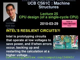
inst.eecs.berkeley.edu/~cs61cUCB CS61C : Machine StructuresLecture 25CPU design (of a single-cycle CPU)2010-03-29 Hello to Valon Mehmetifrom Macedonia! Lecturer SOE Dan Garcia Intel is prototyping circuits that operate at low voltages to save power, and if/when errors occur, backing up and restarting the calculation at a higher voltage… Intel’s Resilient circuits?! technologyreview.com/computing/24843/
Review • CPU design involves Datapath, Control • Datapath in MIPS involves 5 CPU stages • Instruction Fetch • Instruction Decode & Register Read • ALU (Execute) • Memory • Register Write
rd instruction memory PC registers rs Data memory ALU rt +4 imm opcode, funct Controller Datapath Summary • The datapath based on data transfers required to perform instructions • A controller causes the right transfers to happen
How to Design a Processor: step-by-step • Analyze instruction set architecture (ISA) datapathrequirements • meaning of each instruction is given by the register transfers • datapath must include storage element for ISA registers • datapath must support each register transfer • Select set of datapath components and establish clocking methodology • Assemble datapath meeting requirements • Analyze implementation of each instruction to determine setting of control points that effects the register transfer. • Assemble the control logic
31 26 21 16 11 6 0 op rs rt rd shamt funct 6 bits 5 bits 5 bits 5 bits 5 bits 6 bits 31 26 21 16 0 address/immediate op rs rt 6 bits 5 bits 5 bits 16 bits 31 26 0 op target address 6 bits 26 bits Review: The MIPS Instruction Formats • All MIPS instructions are 32 bits long. 3 formats: • R-type • I-type • J-type • The different fields are: • op: operation (“opcode”) of the instruction • rs, rt, rd: the source and destination register specifiers • shamt: shift amount • funct: selects the variant of the operation in the “op” field • address / immediate: address offset or immediate value • target address: target address of jump instruction
31 26 21 16 11 6 0 op rs rt rd shamt funct 6 bits 5 bits 5 bits 5 bits 5 bits 6 bits 31 26 21 16 0 op rs rt immediate 6 bits 5 bits 5 bits 16 bits 31 26 21 16 0 op rs rt immediate 6 bits 5 bits 5 bits 16 bits 31 26 21 16 0 op rs rt immediate 6 bits 5 bits 5 bits 16 bits Step 1a: The MIPS-lite Subset for today • ADDU and SUBU • addurd,rs,rt • suburd,rs,rt • OR Immediate: • ori rt,rs,imm16 • LOAD and STORE Word • lw rt,rs,imm16 • sw rt,rs,imm16 • BRANCH: • beq rs,rt,imm16
Register Transfer Language (RTL) • RTL gives the meaning of the instructions • All start by fetching the instruction {op , rs , rt , rd , shamt , funct} MEM[ PC ] {op , rs , rt , Imm16} MEM[ PC ] inst Register Transfers ADDU R[rd] R[rs] + R[rt]; PC PC + 4 SUBU R[rd] R[rs] – R[rt]; PC PC + 4 ORI R[rt] R[rs] | zero_ext(Imm16); PC PC + 4 LOAD R[rt] MEM[ R[rs] + sign_ext(Imm16)]; PC PC + 4 STORE MEM[ R[rs] + sign_ext(Imm16) ] R[rt]; PC PC + 4 BEQ if ( R[rs] == R[rt] ) then PC PC + 4 + (sign_ext(Imm16) || 00) else PC PC + 4
Step 1: Requirements of the Instruction Set • Memory (MEM) • instructions & data (will use one for each) • Registers (R: 32 x 32) • read RS • read RT • Write RT or RD • PC • Extender (sign/zero extend) • Add/Sub/OR unit for operation on register(s) or extended immediate • Add 4 (+ maybe extended immediate) to PC • Compare registers?
Step 2: Components of the Datapath • Combinational Elements • Storage Elements • Clocking methodology
Combinational Logic Elements (Building Blocks) • Adder • MUX • ALU CarryIn A 32 Sum Adder 32 B CarryOut 32 Select A 32 Y MUX 32 B 32 OP A 32 Result ALU 32 B 32
ALU Needs for MIPS-lite + Rest of MIPS • Addition, subtraction, logical OR, ==: ADDU R[rd] = R[rs] + R[rt]; ... SUBU R[rd] = R[rs] – R[rt]; ... ORI R[rt] = R[rs] | zero_ext(Imm16)... BEQ if ( R[rs] == R[rt] )... • Test to see if output == 0 for any ALU operation gives == test. How? • P&H also adds AND, Set Less Than (1 if A < B, 0 otherwise) • ALU follows chap 5
What Hardware Is Needed? (1/2) • PC: a register which keeps track of memory addr of the next instruction • General Purpose Registers • used in Stages 2 (Read) and 5 (Write) • MIPS has 32 of these • Memory • used in Stages 1 (Fetch) and 4 (R/W) • cache system makes these two stages as fast as the others, on average
What Hardware Is Needed? (2/2) • ALU • used in Stage 3 • something that performs all necessary functions: arithmetic, logicals, etc. • we’ll design details later • Miscellaneous Registers • In implementations with only one stage per clock cycle, registers are inserted between stages to hold intermediate data and control signals as they travels from stage to stage. • Note: Register is a general purpose term meaning something that stores bits. Not all registers are in the “register file”.
Storage Element: Idealized Memory • Memory (idealized) • One input bus: Data In • One output bus: Data Out • Memory word is found by: • Address selects the word to put on Data Out • Write Enable = 1: address selects the memoryword to be written via the Data In bus • Clock input (CLK) • The CLK input is a factor ONLY during write operation • During read operation, behaves as a combinational logic block: • Address valid Data Out valid after “access time.” Write Enable Address Data In DataOut 32 32 Clk
Write Enable Data In Data Out N N clk Storage Element: Register (Building Block) • Similar to D Flip Flop except • N-bit input and output • Write Enable input • Write Enable: • negated (or deasserted) (0): Data Out will not change • asserted (1): Data Out will become Data In on positive edge of clock
Storage Element: Register File • Register File consists of 32 registers: • Two 32-bit output busses: busA and busB • One 32-bit input bus: busW • Register is selected by: • RA (number) selects the register to put on busA (data) • RB (number) selects the register to put on busB (data) • RW (number) selects the register to be writtenvia busW (data) when Write Enable is 1 • Clock input (clk) • The clk input is a factor ONLY during write operation • During read operation, behaves as a combinational logic block: • RA or RB valid busA or busB valid after “access time.” RW RA RB Write Enable 5 5 5 busA busW 32 32 32-bit Registers 32 busB Clk 32
Step 3: Assemble DataPath meeting requirements • Register Transfer Requirements DatapathAssembly • Instruction Fetch • Read Operands and Execute Operation
Next Address Logic Address Instruction Memory 3a: Overview of the Instruction Fetch Unit • The common RTL operations • Fetch the Instruction: mem[PC] • Update the program counter: • Sequential Code: PC PC + 4 • Branch and Jump: PC “something else” clk PC Instruction Word 32
3b: Add & Subtract • R[rd] = R[rs] op R[rt] (addurd,rs,rt) • Ra, Rb, and Rw come from instruction’s Rs, Rt, and Rd fields • ALUctr and RegWr: control logic after decoding the instruction • … Already defined the register file & ALU 31 26 21 16 11 6 0 op rs rt rd shamt funct 6 bits 5 bits 5 bits 5 bits 5 bits 6 bits Rd Rs Rt ALUctr RegWr 5 5 5 busA Rw Ra Rb busW 32 Result 32 32-bit Registers ALU 32 32 busB clk 32
Peer Instruction • We should use the main ALU to compute PC=PC+4 • The ALU is inactive for memory reads or writes. 12 a) FF b) FT c) TF d) TT
How to Design a Processor: step-by-step • 1. Analyze instruction set architecture (ISA) datapathrequirements • meaning of each instruction is given by the register transfers • datapath must include storage element for ISA registers • datapath must support each register transfer • 2. Select set of datapath components and establish clocking methodology • 3. Assembledatapath meeting requirements • 4. Analyze implementation of each instruction to determine setting of control points that effects the register transfer. • 5. Assemble the control logic (hard part!)