3d reverse engineering process
For PCB Board Cloning Service, you can get in touch with us. Our PCB Copy Service is quite popular in the electronics industry. It will allow you to achieve you business goals and make the most out of your available resources. Our Printed Circuit Board Clone is quite popular in the industry and will allow you to achieve the required success in life. The Electronic PCB Board Cloning service will also allow you to make things a lot easier for you. The Circuit Board Cloning service will also make it easier for you to get things done in the most perfect way

3d reverse engineering process
E N D
Presentation Transcript
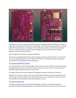
Organization is the key to reverse engineering computed tomography PCB board efficiency, and lack of organization will reduce the efficiency of our PCB design reverse engineering. Take printed circuit board gerber file relayouting rules as an example: when starting a new project, many PCB design engineers tend to reinvent the design according to their own design rules, rather than relying on a proper, organized, systematic approach to rules. Reverse Engineering Computed Tomography PCB Board This practice can significantly slow down project progress when time is of the essence. This article will discuss rule-based approaches that can improve the efficiency of multilayer Computed Tomography circuit board schematic diagram reverse engineering. 3d reverse engineering process It is common practice to recreate PCB design rules for each new project underway. This may be because the design department does not yet have a process in place to reuse the rules, or simply because the PCB design engineer does not want to reuse the rules. The design cloning rules for each Computed Tomography multilayer circuit board are different. Whatever the reason, this points to the need to update design workflows to improve design efficiency and consistency. Without improvements and enhancements, current workflows can take a lot of extra time and effort, and inconsistencies can lead to inheritance issues. IC reverse engineering The design cloning rules for each Computed Tomography multilayer circuit board are different. Generally, we expect PCB design engineers to fully understand the rules and be able to enter the same
values in every design. However, even if their memory is correct, there is always the possibility of entering wrong values. Successful Satellite Communication PCB Board Schematic Diagram Cloning requires careful attention to every step and every detail throughout the PCB board reverse engineering process, which means thorough and careful planning at the beginning of the high frequency printed circuit board design cloning phase, and a comprehensive and continuous evaluation of the progress of each design step. redesign PCB circuit board Satellite Communication PCB Board Schematic Diagram Cloning requires careful attention to every step and every detail throughout the PCB board reverse engineering process And this kind of meticulous design skills is what most electronic enterprise cultures lacked. In recent years, due to the demand and growth of Bluetooth devices, wireless local area network (WLAN) devices, and mobile phones, the industry has paid more and more attention to the skills of RF circuit schematic diagram cloning. From the past until now, radio frequency circuit board design cloning has always been the most difficult part for engineers to control, even a nightmare, just like electromagnetic interference (EMI) problems. Satellite Communication PCB Board Schematic Diagram Cloning right the fSatellite Communication PCB Board Schematic Diagram Cloning requires careful attention to every step and every detail throughout the PCB board reverse engineering process And this kind of meticulous design skills is what most electronic enterprise cultures lacked. In recent years, due to the demand and growth of Bluetooth devices, wireless local area network (WLAN) devices, and mobile phones, the industry has paid more and more attention to the skills of RF circuit schematic diagram cloning. remanufacture printed circuit board From the past until now, radio frequency circuit board design cloning has always been the most difficult part for engineers to control, even a nightmare, just like electromagnetic interference (EMI) problems. Satellite Communication PCB Board Schematic Diagram Cloning right the first time requires careful planning and attention to detail to be effective.irst time requires careful planning and attention to detail to be effective. satellite communication circuit board gerber file reverse engineering Radio frequency (RF) circuit board design is often described as a “black art” because there are still many uncertainties in theory. But this is only a partial view, and there are still many rules that can be followed in RF circuit board design. In actual design, however, the real trick is how to trade off these laws when they cannot be implemented due to various constraints. PCB board clone Important RF design topics include: Impedance and Impedance Matching, Insulator Materials and Laminates, Wavelength and Harmonics…etc. In the development process of WiFi products, the wiring of radio frequency circuits (RF Circuit Layout Guide) is a very critical process. In many cases, we may have a
perfect design in principle, but in the actual board manufacturing, it is found that it is not ideal after the upper part. In fact, these are the reasons why the layout (Layout) is not perfect.