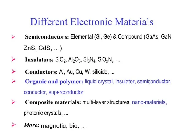
MSE 141 Electronic Materials
MSE 141 Electronic Materials. Electrical Conduction in Materials Dr. Benjamin O. Chan Associate Professor January 2012. Electrons in a Crystal. How are the electrons distributed among the available energy levels? Probabilistic distribution expected

MSE 141 Electronic Materials
E N D
Presentation Transcript
MSE 141 Electronic Materials Electrical Conduction in Materials Dr. Benjamin O. Chan Associate Professor January 2012
Electrons in a Crystal • How are the electrons distributed among the available energy levels? • Probabilistic distribution expected • We can never specify the location and kinetic energy of each individual electron (out of ~ 1022 cm-3) • Fermi Distribution • Applies to fermions • Pauli Exclusion Principle applies • Bosons require Bose-Einstein distribution
Fermi Distribution Function • kB = Boltzmann’s constant = 8.616 x 10⁻⁵eV/K • EF = Fermi energy • Metals: Highest occupied energy at T = 0 K • Semiconductors: energy level with a 0.5 probability of occupation • chemical potential • T = absolute temperature
Fermi Distribution Function (T=0 K) • Ground State • T = 0 K • E = EF • Satisfactory for Metals • For semiconductors, EF is usually in the energy gap: these energies have no chance of being occupied!
Fermi Distribution Function (T>0 K) • At room temperature, DE~1% • For E >> EF • Boltzmann tail
Density of States • Distribution of energy levels over a band • Consider lower part of valence band (e.g. 4s for Cu) • Electrons essentially free • Assume electrons are confined in a square potential well • where nx, ny and nz are the principal quantum numbers and a is now the length of the crystal
Quantum Number Space • nx, ny and nz specify an energy state En • If we take n to be the radius of a sphere containing quantum numbers • The surface of the sphere will contain states yielding the same En
Number of Quantum States • All points inside sphere represent states with E < En • Number of states with E En is proportional to the volume of the sphere with radius n • Only the positive octant and integral values of nx, ny and nz are allowed
DOS Z(E) within a Band • Density of states (DOS) = number of energy states per unit energy • where V = a3 is the volume occupied by the electrons
Some notes on DOS • E vs Z(E) graph • Not the usual Z vs E ! • Parabolic graph • Lower end of the band has fewer available E values compared to higher energies • Area within the curve = number of states with E En • Element area d = Z(E)dE
Population Density • Pauli exclusion principle • 2 electrons of opposite spin per state • Number of electrons per unit energy N(E) • Where F(E) is the Fermi distribution function • N(E) = population density
Population Density N(E) • As T0 and E<EF, N(E)=2Z(E) • T0 and E<EF, N(E) is smeared out • Area within the curve = number of electrons, N*, that have an energy E<En • For an energy interval E to E + dE
Calculating EF • For T0 and E<EF • Defining N’= number of electrons per unit volume and solving for EF, we get • Note: N* does not change with T
Crystal Z(E) within FBZ • For low E, constant energy curves are circles • Free-electron-like • Z(E) is parabolic • For larger energies, Z(E)0 as FBZ boundary is reached • Largest number of energy states available is near the center of a band
Consequences of Band Model • Solids in which the highest filled band is completely occupied by electrons are insulators • Including s-band? • Alkali metals (monovalent) have half-filled valence band • Bivalent metals should be insulators • Closed s-shell • Semiconductor • 4 valence electrons: valence band full!
Bivalent Metal • Is it insulating or conducting? • p band overlaps with s band • Weak binding forces of valence electrons on their atomic nuclei • Upper s band electrons empty into low levels of p band • Partially filled energy bands: metal! • Semi-metal • Are alkali metals more conducting than bivalent metals?
Effective Mass • Empirical evidence shows that mass of electron in a crystal can be larger or smaller compared to the mass of a free electron • We’ll call this the effective mass m* of the electron • m*/mo describes deviation from mo • Usually bigger than 1 (so what?) • Determine an expression for m*
Velocity of an electron in an energy band • Wave packet velocity given angular velocity w and wavenumber k • Acceleration a • For a free electron • This gives us
Effective Mass • Substituting, • Applying Newton’s Second Law • Comparing the two previous equations • m* is inversely proportional to the curvature of the energy band!!
Energy Band Structures Revisited • High curvature = low mass • Low curvature = high mass • Usually at the center or boundary of a BZ • m*/mo can be as low as 1% • Multiple curves for same k leads to multiple values for effective mass • More than one type of carrier available!
More Notes on Energy Band Diagrams • Ideal electron band within FBZ • Calculate first derivative and reciprocal of second derivative • m* is small and positive near center of FBZ and increases for larger values of k • Electrons in the upper part have a negative mass • Defect electron/ electronhole • Particle travels opposite to an electron under an applied electric field • Important in semiconductors • Effective mass is a tensor!
Problem Set 2 • Hummel, 3rd edition • Chapter 6 • 5, 8, 12 • Chapter 7 • 1, 3, 8, 9 • Due Jan. 26, 2012
Electrical Conduction in Metals and Alloys • Electrical Conductivity • The ability of materials to let charge carriers move through it • Units: Siemens/m = 1/Wm • Resistivity is the inverse (Wm) • Insulators/Dielectrics • Unable to conduct electricity • High resistivity
Current Density and Electric Field • Current Density • Flow of charge per unit time per unit area • Units: A/m2 • Electric Field • Region of influence of a charge carrier • Units: V/m • In general, the relationship between the current density j across a material to the applied electric field e across it is • Where s is called the conductivity of the material • This equation does not assume s to be constant!
Ohm’s Law • If s is constant, we get the general form of Ohm’s Law • Hey, nothing changed!! • It’s true the equation did not change externally, but s suffered a transformation, from being a function to becoming constant
A l Ohm’s Law • Consider the material to be a cylinder of length l and cross-sectional area A • Substituting into Ohm’s law equation, • Solving for I,
Conductance G • Defining the conductance G to be • Ohm’s Law becomes • If we set G=1/R, R being the resistance of the material, we get • Or, the more familiar form is
Resistance and Resistivity • The resistance R of the material is then defined as • with r=1/s, the resistivity of the material • R is due to collisions with lattice atoms • Crystal defects tend to increase R • More collisions take place! • Particle Picture
Wave Picture of R • R is due to scattering of charge carriers by atoms • Atoms absorb energy of incoming wave and re-emit them in the form of spherical waves • Treat atoms as oscillators • Periodic structures: waves propagating in the forward direction are “in-phase” (constructive interference) • electron wave passes without hindrance through crystal (coherent scattering) • Non-periodic structures: incoherent scattering
CAUTION! • R, G, r and s (while being constant) are temperature dependent! • R tends to increase (G decreases) with increasing T • What exceptions can you think of?
Classical Electrical Conduction Theory • Pre-QM period • Drude: consider the valence electrons (in a metal) as a gas or plasma • Monovalent atoms contribute one electron per atom • Na=number of atoms=number of charge carriers=N • Where No is Avogadro’s number, d the density of the material and M is the atomic mass (monatomic crystal)
Free Electron Motion • Electrons are accelerated by an applied electric field • For constant e, acceleration is constant • v builds up to infinity! • When e=0, v = constant • This can happen only in superconductors! • This is not what we observe…
Electron Path Through the Conductor • Electrons suffer intermittent collisions with lattice ions
Effect of Collisions • Drag: let g = damping coefficient • Steady state case dv/dt = 0 where vf = drift velocity
Electron Velocity • Modified Differential Equation • Solution • Average time between collisions t
Conductivity and t • Current density • Conductivity • Conductivity is large for large N and t • Mean free path l
Effect of Temperature and Lattice Defects • As T increases, atoms vibrate more about their equilibrium positions • t decreases and s decreases • More collision sites (specially for point and line defects) • t decreases and s decreases
Quantum Mechanical Considerations • Plot velocities in velocity space • Momentum space • k-space • Since there is no preferential velocity, the range of velocities form a disk with radius vF • vF = Fermi velocity, the maximum velocity the electrons can assume • In 3-D, the velocity distribution forms a sphere, the surface of which we call a Fermi surface
More on Velocity… • At equilibrium, all points inside the Fermi sphere are occupied • Velocities cancel each other out resulting in zero net velocity for the whole group • Under an applied electric field, the Fermi sphere is displaced opposite the field direction • Net velocity gain results • Great majority of electrons still cancel each other pair-wise • Uncompensated electrons cause the observed current
So? • Not all conduction electrons contribute to current • Their drift velocity is very close to the Fermi velocity (which is relatively high!) • Classical Mechanics assumes that all conduction electrons contribute to current and move with a modest velocity • How do you compare vf and vF?
Population Density • There are more electrons near EF • Only a little energy DE is needed to raise a substantial number of electrons into slightly higher states • Velocity of excited electrons only slightly higher than vF • Mean velocity remains vF