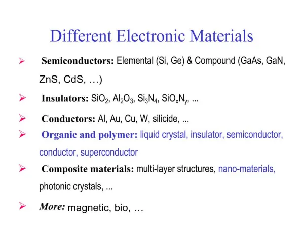
Electronic Materials
Electronic Materials. An Overview R. Lindeke. View of an Integrated Circuit. (a). (d). Al. (d). Si . (doped). 45 m m. 0.5 mm. (b). (c). • Scanning electron microscope images of an IC:. • A dot map showing location of Si (a semiconductor): -- Si shows up as light regions.

Electronic Materials
E N D
Presentation Transcript
Electronic Materials An Overview R. Lindeke
View of an Integrated Circuit (a) (d) Al (d) Si (doped) 45mm 0.5mm (b) (c) • Scanning electron microscope images of an IC: • A dot map showing location of Si (a semiconductor): -- Si shows up as light regions. • A dot map showing location of Al (a conductor): -- Al shows up as light regions. !courtesy Nick Gonzales, National Semiconductor Corp., West Jordan, UT.) Fig. (a), (b), (c) from Fig. 18.0, Callister 7e.
Electrical Conduction • Ohm's Law: DV = I R voltage drop (volts = J/C) C = Coulomb resistance (Ohms) current (amps = C/s) A - (cross e I sect. DV area) L • Resistivity, r and Conductivity, s: -- geometry-independent forms of Ohm's Law -- Resistivity is a material property & is independent of sample resistivity (Ohm-m) E: electric field intensity J: current density • Resistance: conductivity
Electrical Properties • Which will conduct more electricity? • Analogous to flow of water in a pipe • So resistance depends on sample geometry, etc. D 2D
J = (V/ ) Electron fluxconductivityvoltage gradient Definitions Further definitions J= <= another way to state Ohm’s law J current density electric field potential = V/ or (V/ ) • Current carriers • electrons in most solids • ions can also carry (particularly in liquid solutions)
Conductivity: Comparison CERAMICS Soda-lime glass 10 -9 Concrete 10 -13 Aluminum oxide <10 SEMICONDUCTORS POLYMERS -14 -4 Polystyrene <10 Silicon 4 x 10 -15 -10 -17 -11 0 Polyethylene 10 -10 -10 Germanium 2 x 10 -6 GaAs 10 insulators semiconductors -1 -1 • = ( - m) • Room T values (Ohm-m) METALS conductors 7 Silver 6.8 x 10 7 Copper 6.0 x 10 7 Iron 1.0 x 10 Selected values
Example: Conductivity Problem 100m < 1.5V 2.5A 7 -1 6.07 x 10 (Ohm-m) What is the minimum diameter (D) of the wire so that DV < 1.5 V? 100m - e I = 2.5A + - Cu wire DV Solve to get D > 1.87 mm
Electronic Band Structures Adapted from Fig. 18.2, Callister 7e.
Band Structure • Valence band – filled – highest occupied energy levels • Conduction band – empty – lowest unoccupied energy levels Conduction band valence band Adapted from Fig. 18.3, Callister 7e.
- + - Energy Energy empty band empty GAP band partly filled filled valence valence band band filled states filled states filled filled band band Conduction & Electron Transport • Metals (Conductors): -- Thermal energy puts many electrons into a higher energy state. • Energy States: -- for metals nearby energy states are accessible by thermal fluctuations.
Energy States: Insulators & Semiconductors • Semiconductors: -- Higher energy states separated by smaller gap (< 2 eV). Energy Energy empty empty band band ? GAP GAP filled filled valence valence band band filled states filled states filled filled band band • Insulators: -- Higher energy states not accessible due to gap (> 2 eV).
Charge Carriers Adapted from Fig. 18.6 (b), Callister 7e. Two charge carrying mechanisms Electron – negative charge Hole – equal & opposite positive charge Move at different speeds - drift velocity Higher temp. promotes more electrons into the conduction band as T Electrons scattered by impurities, grain boundaries, etc.
6 r Cu + 3.32 at%Ni 5 Ohm-m) Cu + 2.16 at%Ni 4 Resistivity, deformed Cu + 1.12 at%Ni 3 -8 Cu + 1.12 at%Ni 2 (10 1 “Pure” Cu 0 -200 -100 0 T (°C) Metals: Resistivity vs T, Impurities • Imperfections increase resistivity -- grain boundaries -- dislocations -- impurity atoms -- vacancies These act to scatter electrons so that they take a less direct path. • Resistivity increases with: -- temperature -- wt% impurity -- %CW = thermal + impurity + deformation (from J.O. Linde, Ann. Physik5, p. 219 (1932); and C.A. Wert and R.M. Thomson, Physics of Solids, 2nd ed., McGraw-Hill Book Company, New York, 1970.)
Adapted from Fig. 18.9, Callister 7e. 180 50 r 160 Ohm-m) 40 140 125 30 30 120 Resistivity, Yield strength (MPa) -8 20 100 (10 21 wt%Ni 10 80 0 60 0 10 20 30 40 50 0 10 20 30 40 50 wt. %Ni, (Concentration C) wt. %Ni, (Concentration C) From step 1: CNi = 21 wt%Ni Estimating Conductivity • Question: -- Estimate the electrical conductivity of a Cu-Ni alloy that has a yield strength of 125 MPa.
Energy s electrical conductivity, empty -1 band ? (Ohm-m) GAP 4 10 electrons can cross gap at higher T 3 10 filled valence 2 10 band filled states 1 10 filled 0 10 pure band (undoped) -1 10 material Si Ge GaP CdS band gap (eV) 1.11 0.67 2.25 2.40 -2 10 1 000 10 0 50 T(K) Selected values. Pure Semiconductors: Conductivity vs T • Data for Pure Silicon: -- s increases with T -- opposite to metals (from G.L. Pearson and J. Bardeen, Phys. Rev. 75, p. 865, 1949.)
• Concept of electrons and holes: valence electron hole electron hole Si atom electron pair creation pair migration - - + + no applied applied applied • Electrical Conductivity given by: 3 # holes/m hole mobility 3 electron mobility # electrons/m Conduction in Terms of Electron and Hole Migration electric field electric field electric field
Intrinsic vs Extrinsic Conduction hole 4 + 4 + 4 + 4 + 4 + 4 + 4 + 4 + conduction electron 4 + 4 + 4 + 4 + 4 + 4 + • n-type Extrinsic: (n >> p) • p-type Extrinsic: (p >> n) valence 4 + 4 + 4 + 4 + 4 + 4 + 4 + 4 + electron Phosphorus atom Boron atom Si atom 5+ 3 + no applied no applied electric field electric field • Intrinsic: # electrons = # holes (n = p) --case for pure Si • Extrinsic: --n ≠ p --occurs when impurities are added with a different # valence electrons than the host (e.g., Si atoms)
p-n Rectifying Junction p-type n-type + - + - + + - - + - p-type - n-type + + + - + - - + - - + n-type - p-type + + - - + + - + - + - • Allows flow of electrons in one direction only (e.g., useful to convert alternating current to direct current. • Processing: diffuse P into one side of a B-doped crystal. • Results: --No applied potential: no net current flow. --Forward bias: carrier flow through p-type and n-type regions; holes and electrons recombine at p-n junction; current flows. --Reverse bias: carrier flow away from p-n junction; carrier conc. greatly reduced at junction; little current flow.
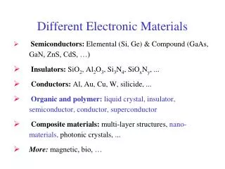
Intrinsic Semiconductors • Pure material semiconductors: e.g., silicon & germanium • Group IVA materials • Compound semiconductors • III-V compounds • Ex: GaAs & InSb • II-VI compounds • Ex: CdS & ZnTe • The wider the electronegativity difference between the elements the wider the energy gap.
• Comparison:intrinsic vs extrinsic conduction... -- extrinsic doping level: 1021/m3 of a n-type donor impurity (such as P). -- for T < 100 K: "freeze-out“, thermal energy insufficient to excite electrons. -- for 150 K < T < 450 K: "extrinsic" -- for T >> 450 K: "intrinsic" 4 10 0.0052at%B s 3 10 -1 2 doped 10 0.0013at%B 1 10 (Ohm-m) electrical conductivity, doped 0 (S.M. Sze, Semiconductor Devices, Physics, and Technology, Bell Telephone Laboratories, Inc., 1985.) undoped 10 pure 3 (undoped) -1 10 2 extrinsic freeze-out intrinsic -2 10 concentration (1021/m3) conduction electron 1 000 10 0 50 1 T(K) 0 0 200 400 600 T (K) Doped Semiconductor: Conductivity vs. T • Data for Doped Silicon: -- s increases doping -- reason: imperfection sites lower the activation energy to produce mobile electrons. (from G.L. Pearson and J. Bardeen, Phys. Rev. 75, p. 865, 1949.)
Number of Charge Carriers Intrinsic Conductivity = n|e|e+ p|e|e • for intrinsic semiconductor n = p • = n|e|(e+ n) • Ex: GaAs For GaAs n = 4.8 x 1024 m-3 For Si n = 1.3 x 10¹⁶ m-3
Transistor MOSFET • MOSFET (metal oxide semiconductor field effect transistor)
Integrated Circuit Devices • Integrated circuits - state of the art ca. 50 nm line width • 1 Mbyte cache on board • > 100,000,000 components on chip • chip formed layer by layer • Al is the “wire”
Ferroelectric Ceramics Ferroelectric Ceramics are dipolar below Curie TC = 120ºC • cooled below Tc in strong electric field - make material with strong dipole moment Fig. 18.35, Callister 7e.
Piezoelectric Materials Piezoelectricity – application of pressure produces current at rest compression induces voltage applied voltage induces expansion
Summary • Electrical conductivity and resistivity are: -- material parameters. -- geometry independent. • Electrical resistance is: -- a geometry and material dependent parameter. • Conductors, semiconductors, and insulators... -- differ in accessibility of energy states for conductance electrons. • For metals, conductivity is increased by -- reducing deformation -- reducing imperfections -- decreasing temperature. • For pure semiconductors, conductivity is increased by -- increasing temperature -- doping (e.g., adding B to Si (p-type) or P to Si (n-type).