Download
1 / 17
170 likes | 189 Vues
This article presents the characterization of a strip crystal previously used at FNAL, including morphological and structural analysis using optical interferometry, RBS-channeling, and XRD. The results indicate the need for further improvement in crystal quality for use in energy measurements at FNAL.

E N D
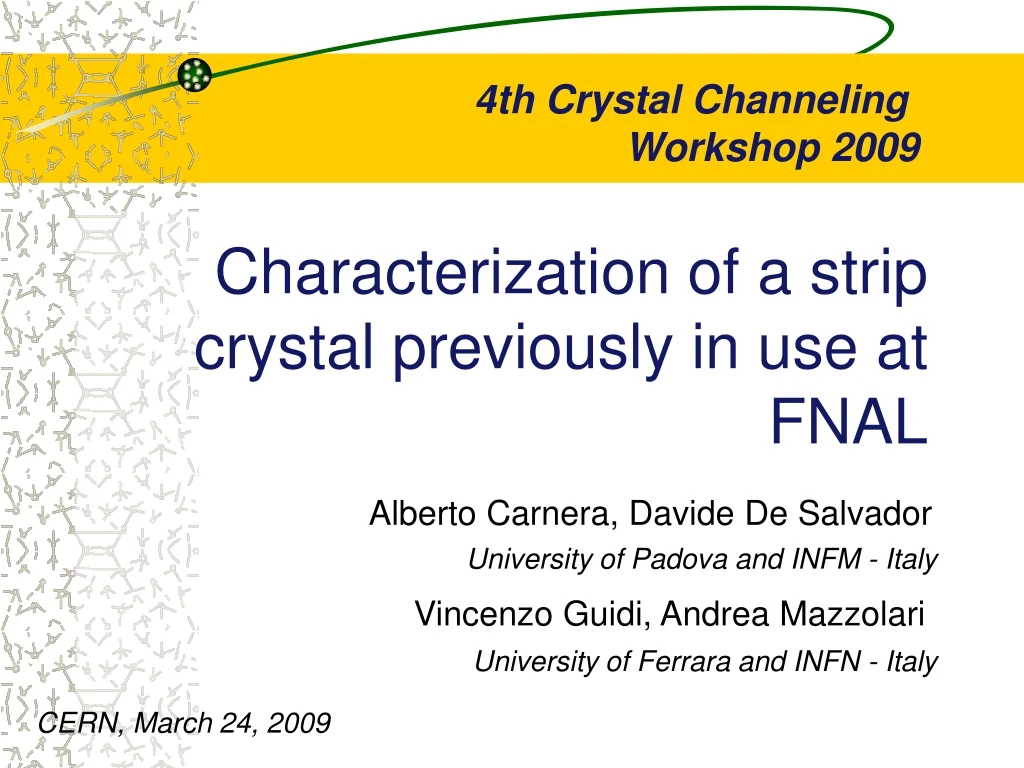
Characterization of a strip crystal previously in use at FNAL 4th Crystal Channeling Workshop 2009 Alberto Carnera, Davide De Salvador University of Padova and INFM - Italy Vincenzo Guidi, Andrea Mazzolari University of Ferrara and INFN - Italy CERN, March 24, 2009
Outlook • Morphological characterization: optical interferometry and AFM • Structural characterization:RBS-channeling and XRD • Characterization of a strip crystal previously in use at FNAL • Conclusions
Crystal bending • Crystal bending is accomplished through anticlastic deformation Principal to anticlastic radii Angle θ (degrees)
Optical characterization • Optical profilometry with 2 nm resolution • Determination of the primary and anticlastic curvatures • Correction of torsion
Planarity and roughness of lateral faces An application of crystals would be the collimation of beam halo in next generation of hadron machines (e.g. the LHC) Particles in the halo drift outwards at the rate of ~2 nm per turn. Since the tune is not integer, the particles will hit the crystal every ~10-20 turns and thereby the first impact parameter of the particles onto the crystal will be in the range of ~100 nm
Planarity and roughness of lateral faces It is demands a crystal with a roughness lower than 100 nm on the lateral faces of the crystal • Roughness can be measured by AFM or optical interferometry • Planarity can be measured by optical interferometry Sub-nm roughness was achieved with ACE
Miscut angle by XRD Nominal lying (110) Real lying (110) The angle between the nominal and the real lying of planes is the miscut angle. It should be of the order or less than 1 mrad
The entry face of the crystal The entry face is crucial because it captures the particles for channeling. It can be analyzed by -- HRTEM (locally) -- RBS channeling (globally) High-qualitysurfaces is achieved via anisotropicchemical etching: ST9 Sub-nm roughness was achieved
RBS - channeling mode Rutherford backscattering under channeling mode is a powerful method to investigate the structure of a surface Channeled particles penetrate deeper into the crystal and are more difficult to emerge out of the surface, resulting in a decrease of the current
RBS spectra 4He+ Low signal of backscattered particles means good crystalline quality p Examples of records by anisotropic chemical etching APL 91(2007)061908
Structure of surfaces The surface min is defined as the ratio of the RBS yield under channelling alignment and random condition extrapolated at the surface channel. The higher the degree of crystalline order in the lattice the lower the surface min due to the reduction of dechanneling from the defects in the crystal. Experimental min for a Si (110) crystal with probe particles of 2 MeV. An ideally perfect surface yields min = 2%
Characterization of a sample previously in use at FNAL Subject: Progress made with INTAS Date: Fri, 1 Jul 2005 14:02:26 +0400 Dear Walter, We are glad to inform you that we have managed with INTAS support to perform a nice crystal deflector which is ready for FNAL experiments, with bending of 150 mrad, and which doesn't require further testing before installation into accelerator. The wafer used for this deflector was perfectly polished in Ferrara. [omissis] Best regards, Valery http://mail.ihep.ru/~biryukov/ We retrieved and applied the procedure we used in our lab at that time, namely a wet isotropic planar etching exposed for two minutes
Morphology of the lateral face • No chemical etching was applied at side surfaces as opposed to our methodology • Bending radius on the center = 15.7 m • Torsion = 20 mrad/mm FNAL FE
Morphology of the entry face FE FNAL • FE sample shows knurling due to the blade of the dicer, which are not present in the other • Presence of large “chipping” at the edges, an indication of rough cut of the sample
XRD characterization • Miscut angle of lateral faces was 80 μrad • Mosaicity was determined at the entry face
RBS channeling The quality of the surface is modest, probably not adequate for the energy at FNAL RBS measurements highlighted that the [1-10] axis is 7° out of axis, i.e., rather an unusual value [111] [1-10]
Conclusions • Example of characterization of a strip-like crystal • Characterization of a crystal previously in use at FNAL • The sample shows features that are significantly different than for our methodology • Proposal for experimentation with such a crystal at H8