
Phase-Locked Loop (PLL)
E N D
Presentation Transcript
Phase-Locked Loop (PLL) • Introduction to Phase-locked loop (PLL) • Historical Background • Basic PLL System • Phase Detector (PD)/comparator • Loop Filter (LPF) • An error Amplifier • Voltage Controlled Oscillator (VCO) • PLL Applications
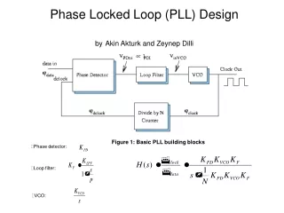
Phase-Locked Loop (PLL) A Phase-Locked Loop (PLL) is a negative feedback system consists of a phase detector, a low pass filter and a voltage controlled oscillator (VCO) within its loop. Its purpose is to synchronize an output signal with a reference or input signal in frequency as well as in phase.
Phase-Locked Loop (PLL) • In the synchronized or “locked” state, the phase error between the oscillator’s output signal and the reference signal is zero, or it remains constant. • If a phase error builds up, a control mechanism acts on the oscillator to reduce the phase error to a minimum so that the phase of the output signal is actually locked to the phase of the reference signal. This is why it is called a PLL.
PLL-Applications The majority of PLL applications fall into four main categories: • Frequency synthesis (Most widely used so PLL is also referred as frequency synthesizer). • Frequency (FM), phase (PM) Amplitude (AM) and modulation and demodulation. • Radar Synchronization & Communication • Data and carrier recovery. • Tracking filters.
PLL-Classification Classification of PLLs: • Analog or Linear PLL (LPLL) • Digital PLL (DPLL) is Analog PLL with digital phase detector • All-Digital PLL (ADPLL) is a digital loop in two senses: all digital components and all digital (discrete-time) signals.
Brief Phase-Locked Loop (PLL) History • 1932: Invention of “coherent communication” using vacuum tube, (deBellescize) • 1943: Horizontal and vertical sweep synchronization in television (Wendt and Faraday) • 1954: Color television (Richman) • 1965: PLL on integrated circuit • 1970: Classical digital PLL • 1972: All-digital PLL • PLLs today: in every cell phone, TV, radio, pager, computer, … • Clock and Data Recovery • Frequency Synthesis • Clock Generation • Clock-skew minimization • Duty-cycle enhancement
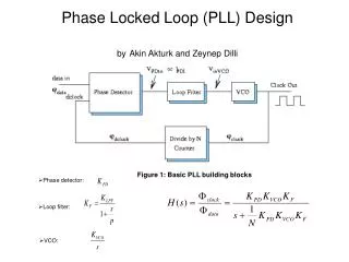
Block Diagram (PLL) The VCO is the free running multivibrator and operates at the set frequency F0 called free running frequency. F0 is determined by external timing components RT and CT. It can be shifted in either side by applying a DC controlled voltage to VOC. The frequency deviation is directly proportional to the DC controlled voltage therefore it is called “Voltage Controlled Oscillator”
Block Diagram (PLL) If the input signal Vs of the frequency Fs is applied to the PLL the Phase Detector compares the phase and frequency of the Fs and VCO output Fo. If the two signals are differ in frequency and/or phase an error voltage Ve is generated. The phase detector is basically a multiplier and produces sum (Fs+Fo) and difference (Fs-Fo)
Block Diagram (PLL) The high frequency signal sum (Fs+Fo) is removed by LPF and low frequency signal difference (Fs-Fo) is then passed by LPF and amplified by an error amplifier which generates the DC control signal Vcfor the VCO to control the Fo. Vcshifts the VCO frequency in either direction so that to reduce the difference between Fs and Fo. Once this action starts we say signal is captured. VCO continues to change theFotill Fo=Fs. The circuit then said to be Locked.
PLL-Capture Transient Once PLL is Locked, it tracks the frequency changes of the input signal Fs. Thus it goes through three stages: Free running Capture Locked or Tracking Above figure shows the capture transient, the LPF controls the Capture range. If the difference signal (Fs-Fo) is too large to pass through the LPF the PLL will not respond. It is said the signal is out of Capture range, but once it is captured PLL can Lock/Track the signal well beyond the capture range. Therefore Tracking Range > Capture Range
PLL: Definitions Lock In Range: Once the PLL is locked, it can track frequency changes in the incoming signals. The range of frequencies over which the PLL can maintain the lock with the incoming signal is called Lock-in Range or Tracking Range and it is expressed as a percentage of Foof VCO frequency. Capture Range: The range of frequencies over which PLL can acquire the lock with an input signal Fs called Capture range and it is expressed as a percentage of Foof VCO frequency. Pull-in Time: The total time taken by PLL to establish the lock is called Pull-in Time. This depends on the initial phase and frequency difference between Fs and Fo, the overall loop gain and filter characteristics.
PLL: Phase Detector/Comparator (Digital) Figure shows the Digital (X-OR) phase detector. Output of X-OR is HIGH only if one of the input signal Fs or Fo is HIGH. This type of Phase detector used only when both the inputs (Fs & Fo) are square wave. The output waveforms when Fs=Foare shown in above figurewhere Fs isleadingtheFobyΦdegrees.
PLL: Phase Detector/Comparator (Digital) Figure shows variation of the DC output voltage (Ve) with Phase difference (Φ). Itshows that the maximum DC output voltage occurs when phase difference is c. Slope of the curve gives the conversion ratio (KΦ) of the phase detector if VCC=5V. KΦ=5V/ π V/rad
VCO- Voltage Controlled Oscillator AVoltage-Controlled Oscillator (VCO) is a circuit that provides a varying output signal (typically of square-wave or triangular-wave form) whose frequency can be adjusted over a range controlled by an externally applied DC voltage. The VCO provides a linear relationship between the applied voltage and the oscillation frequency. The applied voltage is called control voltage. The control of frequency with the help of control voltage is known as voltage to frequency conversion. Hence VCO is otherwise known as Voltage to frequency converter. Practically VCO is available in IC form. IC 566 (LM566/SE566) from Signetics is a popular VCO. IC 566 contains circuitry to generate both square-waveand triangular-wave signals whose frequency is set by an external resistor and capacitor and then varied by an applied dc voltage.
PLL:VCO- Voltage Controlled Oscillator Figure (b) the timing capacitor CT is linearly charged or discharged by a constant current source/sink. The amount of current can be controlled by changing the voltage VC at the modulating input (Pin 5) or by changing the external timing resistor RT.
PLL:VCO- Voltage Controlled Oscillator The voltage at pin 6 is held at same voltage as pin 5. (small capacitor 0.001µF connected between pin 5 & 6 to eliminate possible oscillations) Thus, if VC at pin 5 increased, voltage at pin 6 also increases, results in less voltage drop across RT and thereby decreasing the charging current. VCO commonly used to convert low frequency signals such as ECGs and EEGs into an audio frequency range to transmit over telephone line, 2 way radio communication system or can be recorded.
PLL:VCO- Voltage Controlled Oscillator The voltage at pin 6 is held at same voltage as pin 5. (small capacitor 0.001µF connected between pin 5 & 6 to eliminate possible oscillations) Thus, if VC at pin 5 increased, voltage at pin 6 also increases, results in less voltage drop across RT and thereby decreasing the charging current. VCO commonly used to convert low frequency signals such as ECGs and EEGs into an audio frequency range to transmit over telephone line, 2 way radio communication system or can be recorded.
Features: 1. Wide supply voltage range 10-24V 2. Very Linear Modulation characteristics 3. High temperature stability 4. Excellent power supply rejection 5. 10 to 1 Frequency range with fixed C1 6. The frequency can be controlled by means of current, voltage, resistor or capacitor.
PLL: Low Pass Filter (LPF) The LPF not only removes high frequency components and noise but also controls the dynamic characteristics of the PLL includes Capture range, Lock/Tracking range, Bandwidth and Transient response.
PLL: Low Pass Filter (LPF) Active or passive filters can be individually used of may be in combination. Active filters have following Advantages and Limitations: Advantages: They provide voltage gain and, therefore, can furnish wide control voltage range to the VCO while still maintaining an optimum voltage level for the detector to interface with. As a loop filter, they are capable for providing the high DC gain and low input current. This can result in zero static phase error between Fs and Fo and thus very low error signal energy exist when the loop is locked Limitataions: 1. Active filter contributes noise components that can appear on VCO signal, this troublesome, especially in narrowband FM radios.
PLL: Application-AM Detector The PLL may be used to demodulate AM signal as shown in fig. The PLL is locked to the Carrier frequency of the incoming AM signal. Fo=Carrier Frequency (VCO output). Since the un-modulated AM is fed to the Multiplier through 90º phase shift network as VCO output (Fo) is always 90º phase shifted with incoming AM signal under the locked condition. This makes both the signal applied to the multiplier in same phase.
PLL: Application-AM Detector The output of the multiplier contains both sum (AM+Fo) and difference (AM-Fo) signals, the demodulated output is obtained after filtering high frequency signal by LPF. Therefore, Demodulated output =AM-Fo AM=Fs+Fc VCO locked to Fc therefore Fo=Fc Therefore Demodulated output =Fs+Fc-Fo=Fs
PLL: Application-FM Detector The Un-modulated FM signal (Fc+VmSinωt) and VCO frequency (Fo)whch is locked to the carried frequency (Fc) of the Un-modulated FM signal is given to the Phase detector of PLL. The output of the Phase detector contains both sum (Fo+Fc+VmSinωt) and difference (Fo-Fc+VmSinωt) signals, the demodulated output is obtained after filtering high frequency signal by LPF. Therefore, Demodulated output = Fo-Fc+VmSinωt andVCO locked to Fc, therefore, Fo=Fc Hence Demodulated FM output =VmSinωt
PLL: Application-Frequency translator The Schematic for shifting the frequency of an oscillator by a small factor is shown in the figure. It can be seen that the Mixer (multiplier) and a LPF1 is connected externally to the PLL. The signal Fs which has to be shifted and output frequency Fo of VCO are applied as inputs to the mixer. The output of the mixer contains sum (Fo+Fs) and difference (Fo-Fs). However, the LPF passes only difference (Fo-Fs).
PLL: Application-Frequency translator The translation of Offset frequency F1(where, F1<<Fs) is applied to the phase comparator of the PLL. When PLL is in Locked State, Output of Phase Comparator Sum (Fo-Fs+F1) andDifference (Fo-Fs-F1) LPF2 passes difference component (Fo-Fs-F1) Therefore,Fo-Fs=F1 (Locked) Fo=Fs+F1 Thus it is possible to shift incoming frequency Fs by small factor F1
DAC: R-2-R Ladder (001) DAC: R-2-R Ladder for switch position 001 DAC: Equivalent circuit