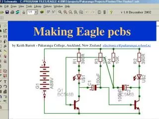
Making Eagle pcbs
v 1.0 December 2002. Making Eagle pcbs. by Keith Barrett - Pakuranga College, Auckland, New Zealand electronics@pakuranga.school.nz. Making Eagle PCBs?.

Making Eagle pcbs
E N D
Presentation Transcript
v 1.0 December 2002 Making Eagle pcbs by Keith Barrett - Pakuranga College, Auckland, New Zealand electronics@pakuranga.school.nz
Making Eagle PCBs? This is the third presentation and will show you how to produce a simple, single layer printed circuit board from a circuit schematic diagram using this software. The circuit schematic for this project can be downloaded as “easy example 1.sch” from: http://www.pakuranga.school.nz/depart/electronics/eaglepcb If you first need to look at preceeding presentations click here to view presentation 1 click here to view presentation 2
How to use this presentation? It would be useful to have access to two adjacent computers. Install and run Eagle on one and this presentation on the other. . Alternatively, print the pages of this presentation and work through them with Eagle running on your PC. .
Loading the Schematic Run the Eagle program, when the control panel window appears click on File > Open >Project . . then find the project folder containing your schematic. You can double click here or here to open the folder. Both actions will load the file for the schematic (and board file if you have already created one)
Creating a Project 2 When the schematic has loaded select File > Switch to board The software will then check to see if a board file exists to go with schematic. If it does it will load the file, otherwise it will offer to create one automatically. select yes
Creating a board 1 This is the component layout generated by the program. components & “wires” Board working area Use the move tool to drag each component onto this area – (this is what will print)
Components can be rotated as well as repositioned Creating a board 2 click on the centre of the symbol to rotate by 90⁰ The next stage is to create the tracks using “autoroute”
Clicking here generates an options menu. . . Creating a board 3 If you are only using single-sided pcbs then set the top layer to N/A . . . then click OK
Autoroute then turns the “wires” into track pathways. . . Creating a board 4
To change the track width, select change > width . . .then select the dimension (these are in inches – units can be set in mm) point at the track and right click. Creating a board 5
To add text select the text tool Creating a board 6 enter text in the box and place on the diagram Text is automatically inverted if the “bottom layer” is chosen
Choose the layers to print select View > Display/hide Creating a board 7
Here you can select what appears on screen and the printer.(blue = selected / white = deselected) Click on the numbers to turn on/off. Click on the colour to edit the colour scheme For most single sided pcbs everything should be off except layers 16,17 (tracks & pads) 45 (drill holes) Save and print your board. Creating a board 8
End of presentation 3 http://www.pakuranga.school.nz/depart/electronics/eaglepcb