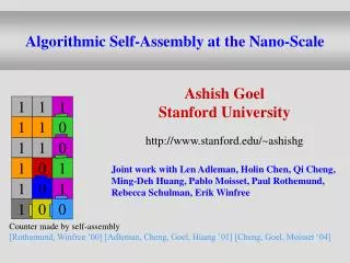
Download
1 / 15
150 likes | 311 Vues
Status of III-V and Nano-Scale Photo-Cathodes at ANL. The “PC-group” @ ANL:. Bernhard Adams Klaus Attenkofer Matthieu Chollet Zeke Insepov Anil Mane Quing Peng. Thomas Prolier Matthew Wetstein Igor Veryovkin Zikri Yusof Alexander Zinovev. Overview. Physics & Technological Challenges

E N D
Status of III-V and Nano-Scale Photo-Cathodes at ANL The “PC-group” @ ANL: Bernhard Adams Klaus Attenkofer Matthieu Chollet Zeke Insepov Anil Mane Quing Peng Thomas Prolier Matthew Wetstein Igor Veryovkin Zikri Yusof Alexander Zinovev
Overview • Physics & Technological Challenges • Different Applications have Different Needs • The Specific Challenge of a Large Photocathode • Technological Challenges: Price, Simplicity, Materials- Process-Compatibility • The Description of the Scientific and Engineering Program • GaN-Family • GaAsP-Family • Nano-Structures • The Path: • Sample Preparation • Characterization • The Goals and “Measure of Success” Large Area Detector Project: 1. Collaboration Meeting
Physics & Technological ChallengesDifferent Applications have Different Needs Hamamatsu: http://jp.hamamatsu.com/products/sensor-etd/pd014/index_en.html • Required spectral response still not clear (main application) • Future applications (combination with scintillators) will require response optimization • III-V are complex to grow, but: • Full developed industry available for production and production tools • Large efforts worldwide in refining growth-technology • This effort can be a milestone for future device development Large Area Detector Project: 1. Collaboration Meeting
Physics & Technological ChallengesThe Specific Challenge of a Large Photocathode • Good conductivity layer to avoid charging effects • Good homogeneity of the cathode over the full size • No “insitu” activation possible -> in vacuum fabrication and sealing necessary • Cathode has to be process compatible to sealing process and final assembly • Cathode has to work under “relaxed” vacuum conditions • The price of the detector will be largely by cathode processing determined • Well established doping methods available • Foundries with large throughput and wafer-sizes available (process parameters can be developed on lab-sizes systems) • High temperature resistivity (about 550C) • Emerging nano-technologies are available • Industrial standards available (yield, homogeneity) III-V are an appropriate approach: http://cqd.eecs.northwestern.edu/research/ebeam.php Large Area Detector Project: 1. Collaboration Meeting
Physics & Technological ChallengesTechnological Challenges: Price, Simplicity, Materials- Process-Compatibility Scalable production tools available http://www.aixtron.com/index.php?id=156&L=1 • Process parameters can be developed on lab-system and transferred to production systems • Complex fabrication (layer-system) will be performed in foundry with quality control • Ready-to-mount cathode (on window) will be transported in air, chemically cleaned and finally brought in the vacuum assembly chamber. • Activation requires high temperature (~600-800C) and small amounts of Cs (sub-monolayer) Large Area Detector Project: 1. Collaboration Meeting
Description of the Scientific & Engineering ProgramPhysics of Semiconductor Cathodes The Three Functions of a Cathode: • Interface layer between window/substrate and active area: • Defines how much light gets into the active light (reflection) • Important for compatibility (growth on glass, bonding, transfer printing….) • Conductivity-layer • Active area: • Light absorption (multilayer options) • Electron transport (scattering/trapping) • Noise-suppression layers • Surface: • Electron escape • Responsible for dark-current • Surface states extreme sensitive to chemical changes Large Area Detector Project: 1. Collaboration Meeting
Description of the Scientific & Engineering ProgramThe Negative Electron Affinity What are surface states: Large Area Detector Project: 1. Collaboration Meeting
Description of the Scientific & Engineering ProgramTunability of III-V • Two “families”: N-based and As-based • Wide tunability of band-gap • Only for specific materials -combinations NEA available • No cross combination of families possible • “Good materials” are direct band gap Large Area Detector Project: 1. Collaboration Meeting
Description of the Scientific & Engineering ProgramGaN-Family Jim Buckley & Daniel Leopold (Wash University) The Challenge • Largest variation in band-gap • Growth on a-Al2O3 (sapphire) • GaN NEA-layer exist • GaN is UV active • Perfect combination would be GaxIn(x-1)N, but:large strain -> high defect density -> large losses • Direct growth on ALD coated a-Al2O3 (sapphire) glass • InN/GaN multilayer system to adjust band-gap and minimize strain • Cascade structures? • Optimizing surface reconstruction (growth direction, temperature, coating) The Research Program Large Area Detector Project: 1. Collaboration Meeting
Description of the Scientific & Engineering ProgramGaAsP-Family The Challenge Xiuling Li and colleagues (UIUC) • Largest family • Growth on GaAs substrate • GaAs too much red! • GaAsP large strain (Similar to GaInN) • Alternative: AlGaAs/GaAs multilayer • No NEA system known for AlGaAs • Finding best bonding or transfer printing technique • Optimizing AlGaAs/GaAs film structure and doping profile • Surface doping & NEA layer • Delta-doping? The Research Program Large Area Detector Project: 1. Collaboration Meeting
Description of the Scientific & Engineering ProgramNano-Structures The Challenge Jonas Johansson (university of Lund) • Largest variety of growth combinations • Radial and longitudinal growth possible • Ion-edging is no issue • Not demonstrated (but various groups have projects) • Growth on glass is possible • Dark current and field enhancement • Developing of a delta-doped radial structure • Most likely GaInN, first test structures GaAs The Research Program Large Area Detector Project: 1. Collaboration Meeting
The Path: Who is involved? • “Bernhard Characterization”: • Bernhard Adams • Matthieu Chollet • Matth Wetstein Common Meetings • People involved (so far): • Klaus Attenkofer • Zeke Insepov • Matth Wetstein • Zikri Yusof • (Thomas Prolier) By Matth Wetstein Berkeley Activity (Ossi) Regular Meeting Characterization Group By Dean Walters • Igor Veryovkin • Alex Zinovev • Potential sample fabrication: • Xiuling Li (UIUC) • Jim Buckley & Daniel Leopold (Wash University) • Jonas Johansson (first samples are waiting for characterization) • “Novosibirsk connection” (Zeke Insepov) • Thomas Prolier (ALD and?) Technical coordination Large Area Detector Project: 1. Collaboration Meeting
The Path: Sample Preparation • Production of “raw-cathode” at collaboration partner (later perhaps also own fabrication capabilities) • Cathode Activation in Argonne (currently work on chamber design) • Compatible to characterization group Standard according Dean Walter • Characterization of: • Quantitative QE(E) • Noise/QE • Field enhancement • Time response Simple thermal coating facility Cs-source Insitu in-plane resistivity Insitu QE-measurement Surface cleaning Chamber: HCL at 1mbar Heating Ni-chamber or glass? Large Area Detector Project: 1. Collaboration Meeting
The Path: Characterization • Characterization: • QE(E) quantitative • Noise/QE • I(EPh,Uexternal,T) (Photo current) • I/µd (Photo current versus absorption) • Calibration of simple light sources • Timing characterization (up to 8/25/50/70GHz?) • Properties: • Transportable • Fully computer controlled • “Bernhard compatible” • “small” optical table • Progress & Status: • Optics components ordered • Electronics components ordered • Calibration diodes available • Data-acquisition system in progress • Current design of vacuum system, chamber, evaporators Large Area Detector Project: 1. Collaboration Meeting
The Goals and “Measure of Success” First Year: • Establishing of collaboration and growth of “small samples (1x1cm2)” • Assembly of high throughput activation/characterization chamber • Automatic data-acquisition and analysis system • Modeling of timing behavior • Demonstration of successful activation of the three cathode systems • Demonstration of QE = 15% for the three cathode systems • GaN • Evaluation of growth on ALD grown Al2O3-films • Demonstration and characterization (dark current/QE) of multilayer approach • Standard NEA-approach • GaAsP • Demonstration and characterization of transfer-printing • AlGaAs/GaAs verus GaAsP evaluation • Investigating NEA-effect and surface reconstruction/coating effects • Nano-structure • Feasibility test (dark current) Large Area Detector Project: 1. Collaboration Meeting