Advanced Yield Prediction Models for Semiconductor Process Improvement
This comprehensive overview explores yield prediction based on design and process models, critical for improving semiconductor fabrication processes. Learn about defectivity and yield models, analysis techniques, defect size distribution, and the impact of outliers on yield projections. Discover key concepts like critical area, Poisson models, and Murphy’s model for accurate prediction of semiconductor yields. Explore the importance of optimizing design and process, and recognize when it’s time to transition to maintaining a cleaner fabrication environment to increase yield efficiency.


Advanced Yield Prediction Models for Semiconductor Process Improvement
E N D
Presentation Transcript
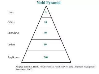
Overview • Yield Prediction • Based on design and the process • Assumes a model for yield loss • Yield loss (for a particular design) • Random defects in the process • sub-optimal process (called “systematic yield loss”) • Why yield prediction? • Used to determine which process needs improvement • Modify designs suitably, if process cannot be improved • Stop working on a process/design, if the maximum possible yield is achieved! • And start on maintaining ‘cleaner’ fab for increasing yield
Index • Defectivity and Yield Prediction • size distribution • density distribution • Yield models • Defectivity, Fail Rate • Defect identification • electrical, optical, FA • Concept of critical area
Index • Test Data (Yield) Analysis • SOF, COF analysis • overlay (inline, e-test, yield, bin) • classification of defects, kill ratio • correlation • Equipment (lot history) • Memory • Repair, redundancy, effect on yield
Defect • Defect Size Distribution (metal,poly...) • less number of Larger defects • Model Parameters (Do,P,Xo) • Outliers, Excursions • Concept of Critical Area • Assume uniform defect density distribution • Point Defects of identical size (Contact, via) • Defect Density distribution (uniform, normal, other models) • Not the same as Defect Size Distribution • Fail Rate
Defect Size Distribution (DSD) • Defects of very small size will not cause shorts /opens • Min space / width causes ‘fails’ • Xo • Defectivity decreases with particle size • Reasonable model: powerlaw Defect Density(#/cm2) Xo Size (mm)
Defect Size Distribution • Values of Do and P • ‘health’ of the fab • Typically p=3 • Typical Do should be 0.5 for a very good fab • why? • Outliers have to be considered separately
Yield Prediction • Very rough idea based on area of chip and Number of metal levels (or number of mask levels) • N is also called ‘complexity’ of the chip • D is the defect level • does not take into account the defect size distribution (large vs small defects) • does not take into account the complexity of design (dense vs sparse etc)
Yield Model Via • For Via or contact • Assume all defects are of identical size (same as that of one via) • One defect kills one via • If defect density is x (number/sq.cm), probability that a location will have that defect density is P(x) • The probability that a location with such a defect density will pass is Y(x) • Total yield • Constraint • Usually, infinity replaced by 10 mm or so
Yield Model Via • If defect density is x, Y(x) is given by • N is the relevant parameter • Number of single via, or Critical Area • Note: Electrically single/redundant via vs Geometrically single/redundant
Poisson Model Via • If defect density is uniform (NOT random) • delta function • Yield = exp(-kN), where k is the fail rate • eg. Test structure has a billion via, 2 opens are detected • Fail rate is 2 ppb • Satisfies the constraint • Poisson Model (Usually used, for its simplicity) • Valid when defectivity is very low • Generally yield predictions may be too pessimistic • Not valid with strong spatial signal • center vs edge or clustering k
SEEDS Model Via • Defect density decreases exponentially • (NOT defect size). All defects are point defects • P(x) = 1/k*exp(-x/k) • 1/k is needed for normalization • Yield = 1/(1+kN) • In general, yield predictions are very optimistic • More accurate, if there are lot of clusters 1/k
Murphy’s Model Via • Triangular (to approximate normal distribution) 1/N • Rectangular 2N 1/2N • Generally not applicable 2N
Gamma Model Via • Empirical • has two parameters (k and alpha) • Covers Poisson model at one end and Seeds model at the other • Alpha is the ‘randomness’ of defects • a =1 (clustered, SEEDS model) • a = infinity (approaches Poisson Model) • a = 4.2 (approx Murphy’s model)
Yield Prediction Metal/Poly • Poisson Model: For metal or poly, the parameter used is ‘critical area’ • A particle of size < ‘s’ will not cause any short (in aluminum process, for example) x L s s s • A particle of size > ‘s’ will cause short only if it falls in the shaded region of width ‘x’ and length ‘L’ • A particle of size =‘s’ will cause short only if it falls on an exact line (Critical area is barely zero)
Yield Prediction Metal/Poly • For each layer, the minimum defect (that can cause fail) may vary • Layout quantities calculated (Layout Extraction) • Electrically redundant (net list) vs isolated
Yield Prediction Metal/Poly • Critical Area vs Defect Size curve Yield Loss • Very small defect ==> No yield loss Critical Area • When defect size approaches that of chip, critical area is the same as the area of the chip Size • Yield Prediction by multiplying critical area and DSD and integrating the result Lower limit (instead of 0,use Xo)
DSD Identification • Optical detection • direct method • model fit to provide Do and P • killer and non killer defects identified • classification/ pareto based on experience • Outlier removal to obtain better model fit • Account for outlier separately (in yield prediction) Density Size
DSD Identification • Electrical Detection • Done on test chips (using yield of test structures) • Better for identifying killer defects • overlay with optical (KLA) provides correlation • KLA done on test chip and Product chip • Not all areas ‘scanned’ optically • Calculation to obtain Do and P (assumes a yield model like Poissson Model) • Min Resolution depends on the space/width of structures • Accuracy depends on the total structures • more structures per die, more wafers... • Use of nest to enhance resolution
Defect Identification • Failure Analysis • Not practical for obtaining defect size distribution • Very useful for determining failure mechanism and in defect classification • Typically Voltage contrast test, FIB (Focussed Ion Beam)
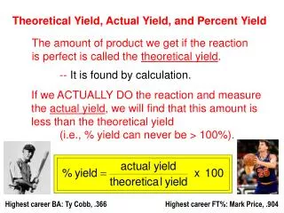
Review • Understanding of Modules • Basics of Testing (to detect defects, process issues and to determine if the product is passing/failing) • Defect distribution Models • Yield Models • Defect detection techniques (basics) • and fit to the model • Missing yet... • How to predict the yield of a chip • and compare with ‘real’ results • and decide on next step (if the prediction is correct vs incorrect)
Yield Prediction • Analyze the whole chip yield • easy • vs process split, by wafer, by lot and so on • Analyze by blocks (sub units) of the chip • Random defect should be the same for all the blocks in a chip • Any deviation must come from different sensitivity of the blocks to various processes
Yield Prediction • Calculate (extract) the critical area, via count, contact count etc... • In general, if the fail rate is 3 ppb and defectivity is 0.5, yield of the chip, based on Poisson Model • Note: Poly, Active shorts are not accounted for • Metal opens excluded • Numbers given are dummy but ‘realistic’
Yield Prediction • Can be done at block level also ROM SRAM • Random defectivity • ==> block yields are independent • multiply each block yield to obtain chip yield • Similarly multiply each layer yield to obtain chip (or block) yield • Memory : Account for Repair!
Yield Data Analysis • Usually SOF test data • Check if ‘random’ model applied • account for known trends (center edge etc) • ‘convert’ to COF data • Isolate block which does not follow trend • Compare with other data • scribe line, inline, optical defect, thickness measurement... • Look for other modes of fail (for layout extractions not accounted for yet)
Yield Data Analysis • Plot wafermap • do the fails look random? • (are the fails caused by random defectivity)? • Any trend (cluster, first wafer effect...) • Extracting ‘COF’ data from ‘SOF’ data • example
Yield Data Analysis • Assume fails are based on random fails • if not, then assume that sub optimal processes affect all the blocks ‘randomly’ • Need sufficient sample size • No correlation between fails for different blocks • If 50 chips are tested and you get the following results.... • which block (test) should be fixed first? And Why?
Yield Data Analysis • If 50 chips are tested and you get the following results.... • Block associated with Test-4 has the lowest yield • Fix • Test-4 • Test-2 • Test-1 • Test-3
Yield Data Analysis • If block yields are correlated • e.g. If one of the tests (Test-3) uses ‘block-2’ structure also • or if the block-2 and block-3 are very similar in design and the ‘unknown’ fail mode is affecting them to the same extent... • All the chips that failed for Test-2 would have failed for Test-3 also • and the table will look like... • Different conclusions!
Yield Data Analysis • To identify block yield correlations • COF for some wafers • Re-order test to ‘estimate’ correlations • More sample size to obtain accuracy • ‘COF like’ data extraction has to be done at wafer level, or lot level • Not at die level! • Compare ‘predicted’ vs ‘real’ ‘COF’ yield for blocks
Yield Data Analysis, Eg1 1 B3 Real Yield B2 B4 B1 0.8 1 Predicted Yield • B1, B2 and B3 yields are ‘as predicted’ (more or less) • B4 yield is much lower than what is predicted • ==> Block-4 is ‘hit’ by a systematic problem
Yield Data Analysis. Eg. 2 1 B4 Real Yield B3 B2 B1 0.8 1 Predicted Yield • All blocks have lower yield than predicted • ==> likely that estimated defect level is optimistic
Yield Data Analysis. Eg 2 • Plot ‘COF’ yield vs critical area/via/contact count (log scale) B4 Real Yield B3 B2 B1 Log (via count...) • Fit a line to obtain Do and FR • More number of blocks is better • Typically too few blocks and too many unknowns (use reasonable estimates)
Yield Data Analysis. • If a block falls ‘away’ from general trend, then likely ‘non random’ issues (OR perhaps Poisson model assumptions are not vaid) • Even if there is not much ‘trust’ in the model or fail rate estimates... • Plot Block-1 ‘COF’ yield vs Block-2 ‘COF’ yield and so on... Block1 yld Not likely to be random Block2 yld
Yield Data Analysis. • If a block has systematic yield loss • or if there are reasons to believe that the whole chip hit by systematic loss... • Need to determine the mode of fail and which module is causing the problem • To obtain better idea • Equipment Commonality (equipment related) • Do all wafers show the issue? Only some wafers? • Inline CD (top/bottom SEM) (process related) • Inline thickness measurement (process related) • scribe line data correlation (mode of fail) • Field Analysis (by shot)
Yield vs Scribe Line. • Scribe line analysis • Scribe line only in some locations • Take the ‘COF like’ yields in the surrounding chips • Otherwise use wafer average • Plot yield vs M3 resistance data (for example) Y R
Yield vs Scribe Line • Scribe line structures are small • ==> small variations/increase in scribe line is likely to represent a larger variation/increase in the product chip • ==> increased M3 resistance or M3 opens a possible issue • If scribe line shows severe opens or shorts, chip will be dead • Example: A chip has 10 million via12 and scribe line has 1000 via12 • For a FR of 10 ppb, chip via12 yield is 91%. Scribe line yield is 99.99% • Very few scribe lines tested vs all chips tested • ==> not likely to see full blown opens/shorts in scribe lines
Yield vs Inline • Similar analysis for Inline data • thickness, CD • SEM CD measurements typically taken in scribe line • usually post etch, sometimes pre etch • can compare with electrical CD • between different products in the same fab • Sometimes there will be (deliberate) difference in the CD, because of difference in target • Thickness by 4 point probe, optical • Note: SEM and Steppers may be linked. Look for commonality • As much as possible, use the dies next to the ‘measurement location’ to calculate ‘COF like’ yield
Yield vs Inline Defectivity • Compare with Inline Defectivity • Overlay defect vs yield map • Classified (pareto) vs yield • ADC (automatic defect classification) • sensitivity, observable defect size ....