Direct Memory Access (DMA)
Direct Memory Access (DMA). Topics to be discussed Basic DMA Concept DMA pins and timing DMA on the 8086 Microprocessor 8237 pins A 8237 DMA application 8237 registers 8237 Software commands. Basic DMA concept

Direct Memory Access (DMA)
E N D
Presentation Transcript
Direct Memory Access (DMA) Microprocessors I -
Topics to be discussed • Basic DMA Concept • DMA pins and timing • DMA on the 8086 Microprocessor • 8237 pins • A 8237 DMA application • 8237 registers • 8237 Software commands Microprocessors I - Frederick University
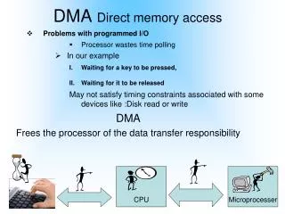
Basic DMA concept • Direct memory access (DMA) is a feature of modern computer systems that allows certain hardware subsystems to read/write data to/from memory without microprocessor intervention, allowing the processor to do other work. • Used in disk controllers, video/sound cards etc, or between memory locations. • Typically, the CPU initiates DMA transfer, does other operations while the transfer is in progress, and receives an interrupt from the DMA controller once the operation is complete. • Can create cache coherency problems (the data in the cache may be different from the data in the external memory after DMA) BACK
BASIC DMA TERMINOLOGY • DMA channel: system pathway used by a device to transfer information directly to and from memory. There are usually 8 in a computer system • DMA controller: dedicated hardware used for controlling the DMA operation • Single-cycle mode: DMA data transfer is done one byte at a time • Burst-mode: DMA transfer is finished when all data has been moved
DMA pins and timing x86 Interrupt Pins • HOLD: DMA request. • Sampled in the middle of any clocking cycle • HLDA: DMA acknowledge signal. • The address, data and control buses are set to high-Z, so the I/O devices can control the system bus BACK
DMA on the 8086 Microprocessor • The I/O deviceasserts the appropriate DRQ signal for the channel. • The DMA controller will enable appropriate channel, and ask the CPU to release the bus so that the DMA may use the bus. The DMA requests the bus by asserting the HOLD signal which goes to the CPU. • The CPU detects the HOLD signal, and will complete executing the current instruction. Now all of the signals normally generated by the CPU are placed in a tri-stated condition (neither high or low) and then the CPU asserts the HLDA signal which tells the DMA controller that it is now in charge of the bus. • The CPU may have to wait (hold cycles). • DMA activates its -MEMR, -MEMW, -IOR, -IOW output signals, and the address outputs from the DMA are set to the target address, which will be used to direct the byte that is about to transferred to a specific memory location. • The DMA will then let the device that requested the DMA transfer know that the transfer is commencingby asserting the -DACK signal. • The peripheral places the byte to be transferred on the bus Data lines. • Once the data has been transferred, The DMA will de-assert the -DACK2 signal, so that the FDC knows it must stop placing data on the bus. • The DMA will now check to see if any of the other DMA channels have any work to do. If none of the channels have their DRQ lines asserted, the DMA controller has completed its work and will now tri-state the -MEMR, -MEMW, -IOR, -IOW and address signals. • Finally, the DMA will de-assert the HOLD signal. The CPU sees this, and de-asserts the HOLDA signal. Now the CPU resumes control of the buses and address lines, and it resumes executing instructions and accessing main memory and the peripherals. BACK
8237 pins • CLK: System clock • CS΄: Chip select (decoder output) • RESET: Clears registers, sets mask register • READY: 0 for inserting wait states • HLDA: Signals that the μp has relinquished buses • DREQ3 – DREQ0: DMA request input for each channel • DB7-DB0: Data bus pins • IOR΄: Bidirectional pin used during programming and during a DMA write cycle • IOW΄: Bidirectional pin used during programming and during a DMA read cycle • EOP΄: End of process is a bidirectional signal used as input • to terminate a DMA process or as output to signal the end of the DMA transfer • A3-A0: Address pins for selecting internal registers • A7-A4: Outputs that provide part of the DMA transfer address • HRQ: DMA request output • DACK3-DACK0: DMA acknowledge for each channel. • AEN: Address enable signal • ADSTB: Address strobe • MEMR΄: Memory read output used in DMA read cycle • MEMW΄: Memory write output used in DMA write cycle BACK Microprocessors I - Frederick University
8237 registers • CAR (Current Address Register): holds the 16-bit memory address used for the DMA transfer (one for each channel), either incremented or decremented during the operation • CWCR (Current Word Count Register): Programs a channel for the number of bytes (up to 64K) transferred during a DMA operation • BA (Base Address) and WC (Word Count): Used when auto-initialization is selected for a channel, to reload the CAR and CWCR when DMA is complete. • CR (Command Register): Programs the operation of the controller BACK
MR (Mode Register): Programs the mode of operation for a 8237 registers channel (one for each channel). • RR (Request Register): Used to request DMA transfer via software (memory-to-memory transfers)
MR (Mask Register): • 8237 registers • SR (Status Register): Shows the status of each DMA channel
8237 Software commands • Clear First/Last Flip-Flop - This command is executedprior to writing or reading new address or word countinformation to the 82C37. This command initializes the flipflopto a known state (low byte first) so that subsequentaccesses to register contents by the microprocessor willaddress upper and lower bytes in the correct sequence. • Set First/Last Flip-Flop - This command will set the flip-flopto select the high byte first on read and write operations toaddress and word count registers. • Master Clear - This software instruction has the same effectas the hardware Reset. The Command, Status, Request,and Temporary registers, and Internal First/Last Flip-Flopand mode register counter are cleared and the Mask registeris set. The 82C37A will enter the idle cycle. • Clear Mask Register - This command clears the mask bitsof all four channels, enabling them to accept DMA requests. • Clear Mode Register Counter - Since only one addresslocation is available for reading the Mode registers, aninternal two-bit counter has been included to select Moderegisters during read operation. To read the Mode registers,first execute the Clear Mode Register Counter command,then do consecutive reads until the desired channel is read.Read order is channel 0 first, channel 3 last. The lower twobits on all Mode registers will read as ones. BACK