Download

1 / 40
410 likes | 598 Vues
Picosecond Timing with Micro-Channel Plate Detectors. Jean-Francois Genat Fast Timing Workshop Lyon, Oct 15 th 2008. Fast Timing Devices. Multi-anodes PMTs Si-PMTs MCPs Dynodes Quenched Geiger Micro-Pores

E N D
Picosecond Timing with Micro-Channel Plate Detectors Jean-Francois Genat Fast Timing Workshop Lyon, Oct 15th 2008
Fast Timing Devices Multi-anodes PMTs Si-PMTs MCPs Dynodes Quenched Geiger Micro-Pores QE 30% 90% 30% CE 90% 70% Rise-time 0.5-1ns 250ps60-200ps TTS (1PE) 150ps 100ps20-30ps Pixel size2x2mm250x50mm21.5x1.5mm2 Dark counts1-10Hz1-10MHz/pixel 1-10 kHz/cm2 Dead time 5ns 100-500ns 1ms Magnetic field noyes 15kG Radiation hardness1kRad=noisex10 Lifetime- ? ~ Coulomb total charge Jean-Francois Genat, Fast Timing Workshop, Lyon, Oct 15th 2008
Micro Channel Plate Detectors MCP Signals Fast Timing Integrated Electronics for fast Timing Conclusion Jean-Francois Genat, Fast Timing Workshop, Lyon, Oct 15th 2008
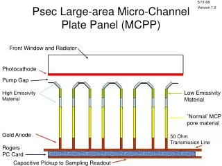
vacuum Micro-Channel Plate Detectors Photo-cathode 200 V 1st gap pores in glass with 2dry emitter 2d gap Basic principle 1- 2kV a few mm 200 V Pore diameter 3-25 mm Pore aspect ratio: 1:50 Anodes (1.6 x 1.6mm2 pixels) Jean-Francois Genat, Fast Timing Workshop, Lyon, Oct 15th 2008
Micro-Channel Plate Detectors The fastest photo-detector to date From Photek Jean-Francois Genat, Fast Timing Workshop, Lyon, Oct 15th 2008
Imaging MCP: Image Charge Technique • Stable charge footprint distribution on the readout • No partition noise – caused by quantisation of charge • No image degradation due to secondary electron effects • Substrate provides electrical isolation • Can always operate anode at ground – lower noise • Intensifier or flange mounted detector - can use external readout • Readouts easily interchanged Timing ~ 1ns !
MCP for Timing and position: Transmission Line Readout Position 1mm Timing: 2.5ps From F. Tang Jean-Francois Genat, Fast Timing Workshop, Lyon, Oct 15th 2008
Transmission Line Readout Position: 1 mm resolution Time: 2.5ps Transmission Line Readout Board From F. Tang Jean-Francois Genat, Fast Timing Workshop, Lyon, Oct 15th 2008
MCP characteristics • Quantum efficiency Photo-cathode, pores geometry, field • Charge gain Pores properties, pores walls material, field • Dark counts Photo-cathode, pores properties • Transit time (rise time) All dimensions,recoil electrons • Ringing Pores geometry, (chevron, curved) • After-pulses “ • Dead-time “ • Lifetime Total charge (Coulombs): • gain in electronics ? Time resolution:Transit Time Spread (TTS) Jean-Francois Genat, Fast Timing Workshop, Lyon, Oct 15th 2008
MCP Device Simulations Pores simulations: David Yu Jean-Francois Genat, Fast Timing Workshop, Lyon, Oct 15th 2008
Micro Channel Plate Detectors MCP Signals Fast Timing Integrated Electronics for fast Timing Conclusion Jean-Francois Genat, Fast Timing Workshop, Lyon, Oct 15th 2008
Measured MCP Signals 2” x 2” MCP, 64 anodes, one single pad Jean-Francois Genat, Fast Timing Workshop, Lyon, Oct 15th 2008
2x2mm2 1”x 1” Beam-Tests: MCP Signals spectra Measured (FNAL MTBF T979 Beam-Tests) Simulated Same noise corner at 1.2 GHz Jean-Francois Genat, Fast Timing Workshop, Lyon, Oct 15th 2008
Micro Channel Plate Detectors MCP Signals Fast Timing with MCPs Integrated Electronics for fast Timing Conclusion Jean-Francois Genat, Fast Timing Workshop, Lyon, Oct 15th 2008
Timing Time spread proportional to rise-time and noise Jean-Francois Genat, Fast Timing Workshop, Lyon, Oct 15th 2008
Fast timing with MCPs MCP level: Dimensions critical Reduce primary and secondary gaps - Transit time reduced Electronics level:Avoid parasitic readout components - Parallel capacitances - Series inductances Reduce Rise-time, consequently improve Time resolution Jean-Francois Genat, Fast Timing Workshop, Lyon, Oct 15th 2008
Multi-threshold Pulse sampling and Waveform analysis Leading edge Constant-fraction Constant fraction Leading edge errors Extrapolated time Advanced Timing techniques Sample, digitize, Fit to the known waveform Jean-Francois Genat, Fast Timing Workshop, Lyon, Oct 15th 2008
Pulse Sampling 2 12 25 80 128 50 32 … Sampling period = 200 ps Timing
Methods compared Matlab simulations (cpp by David Salek) Monte-Carlo: 300 synthesized events Time resolution vs Number of photo-electrons Jean-Francois Genat, Fast Timing Workshop, Lyon, Oct 15th 2008
Beam Tests Check Run the same algorithm using actual MCP beam-tests data taken at the FNAL T979 Meson Beam-Tests Facility Beam tests conditions: - 350 MHz analog bandwidth - 20 GS/s sampling - 8-bit - ~ 10 photo-electrons (?) - 25 mm pores Photonis MCPs 2”x 2” Simulation with synthesized data: 34ps With measurement data: 40ps Jean-Francois Genat, Fast Timing Workshop, Lyon, Oct 15th 2008
Fast Timing Electronics for MCPs MCP Electronics Constant fraction SLAC - NIM 6ps 3.4ps LBNL/Hawaii - Discrete Multi threshold Chicago - Discrete + CERN TDC chip Waveform analysis Hawaii - BLAB line chips 6GS/s 20ps 6.4ps Orsay/Saclay - SAM line 3.2GS/s 25ps PSI - DRS line 5GS/s 3ps ? Under development: - 40 GS/s, multi-GHz range analog bandwidth sampling chip Chicago + Hawaii + Orsay/Saclay Reviews by PSI Jean-Francois Genat, Fast Timing Workshop, Lyon, Oct 15th 2008
Timing with Sampling • Critical parameters: • Detector • - Signal dynamics (NPE, Rise-time, TTS) • - Signal/noise ratio • Sampling device • - Analog bandwidth • - Sampling rate • - Clock jitter • - ADC resolution • - Trigger modes
Micro Channel Plate Detectors MCP Signals Fast Timing Integrated Electronics for fast Timing Conclusion Jean-Francois Genat, Fast Timing Workshop, Lyon, Oct 15th 2008
Fast sampling ASIC architecture Sampler frozen upon input trigger (ext, or channel) On-chip ADC Foreseen technology: CMOS IBM 130nm Jean-Francois Genat, Fast Timing Workshop, Lyon, Oct 15th 2008
Technology IBM 8RF DM 130nm CMOS • Design kit from CERN • Key numbers • 40 GS/s sampling • 1.5 GHz analog bandwidth • Gain • Depth 64-128 • 8 -10 bit ADCs • Self/Global trigger • Time stamp • Blocks: • Input buffer • Discriminator • Delay generator (optional PLL) • Clock buffer • Switched capacitors array • ADC • Control Fast Sampling ASIC
Fast Sampling ASIC Details 16 + 1 channels, 64 cells at 40 GHz Wilkinsons 16 x 64 10-bit ADCs registers and control 16 Inputs SCArray 16 x 64 64 16 thresh sel 16- - - Input buffer Disc 64 16 trigs Ext trig 16 ext_trig Start conv Ramp + buffers delay 64b Vtop Vbtm 16 trigs 6b 16 trigs 500M ck 625 MHz Ck Vernier timing ADC controls lock Analog controls Digital outputs thresh Vtop Vbtm fine time stamps 16 x 6b 10-bit samples Registers and control Storage control 16 trigs 16 trigs Start conv lock ADCs control Output storage <16 time stamps: 6b fine + n-bit coarse + 4 ch <16 x 64 samples: 10-bit Digital controls clk 8data data write/read sel
Delay Locked Loop Time arbiter Clock Delay + time offset controls N delay elements t
640 MHz clock in 16 cells 100ps 100ps 100ps 100ps 125ps 150ps 175ps 16 x 4 = 64 cells, 25ps step delays 40 GS/s Timing generator 0ps Physical Layout critical Jean-Francois Genat, Fast Timing Workshop, Lyon, Oct 15th 2008
MCPs electronics plans at EDG Chicago • Fast sampling chip plans: • Year 1 • 2-channel chip @ 40 GHz • Check with one delay-line channel • - Year 2 • Implement 16-channels to read a full 1024-anode MCP • - IBM 130nm CMOS design kit running on Sun workstations • - Hawaii, Orsay and Saclay are joining Jean-Francois Genat, Fast Timing Workshop, Lyon, Oct 15th 2008
Micro Channel Plate Detectors MCP Signals Fast Timing Integrated Electronics for fast Timing Conclusion Jean-Francois Genat, Fast Timing Workshop, Lyon, Oct 15th 2008
MCPs Readout for 220m AFP - Use self-trigger mode and time stamp - Digitize/process on L1 data in time with L1 - 4 protons/BCO: 4 x 2.5ms / 25ns = 400evts to buffer / L1 latency Caveat: - radiation hardness - lifetime (work at lower HV) TTC device (or GBT) MCP - 40 GHz Sampling - 32-channel x 512-evts x 256-samples analog buffer - Wilkinson ADCs - DSP Transmission lines PCB Jean-Francois Genat, Fast Timing Workshop, Lyon, Oct 15th 2008
MCP MTest T979 (FNAL) Beam-Tests Results 2x2mm2 2”x 2” 1’ Jerry Va’Vra Erik Ramberg Tyler Natoli Henry Frisch Ed May + … 25 mm Burle/Photonis 2” x 2” 1.3-13.9 ps 23 PE (?) 10 mm Burle/Photonis 2” x 2” 14.2-12.4 ps 35 PE (?) 5-6 mm Photek 1cm27.4-8.8 ps 16 PE (?) - 5.6-10mm quartz radiator - Electronics noise (CFD + TAC + ADC) : 6.5 ps (subtracted) Anatoly Ronzhin Silicon PMs: 47 ps
As an Imaging device… Coupling to Board Position: 10mm resolution Time: 1ns Imaging Micro-Channel Plates Detectors Wedge and Strip technique Coupling to ASIC: 3 mm From GLAST, Bellazini et al… NIM 591 2008 From J. Lapington, for WSO, Uni. Leicester, UK
MCP characteristics • Spatial resolution • Fundamentally limited by MCP pore geometry • Pore diameters as low as 2 µm • 2 µm resolution requires centroiding! • Temporal resolution • Small pores • Smaller geometry • Faster pulses • τ= 66 ps, FWHM = 110 ps • Multiple MCPs, pulse saturation slows risetime • Noise • Background • Typically <1.0 cm-2 s-1 • Low noise glass • Reduced Potassium-40 decay • Low noise glass <0.1 cm-2 s-1 • Lifetime • Dependent on extracted charge • Gain plateau from 0.1C/cm2to 1C/cm2 • Equivalent to ~1013 events/cm2
Vernier Anode – enhanced performance geometric charge division • Geometric charge division using 9 electrodes • 3 groups of 3 sinusoidal electrodes • 3 cyclic phase coordinates • Cyclically varying electrodes allow • Determination of a coarse position using a Vernier type technique • Spatial resolution greater than charge measurement accuracy • The full unique range of the pattern can be utilized • Typically 3000 x 3000 FWHM pixel format • Easy to reformat – e.g. 6000 x 1500, etc. • Up to 200 kHz max. global count rate
Tetra Wedge Anode PCB Layer 1 Y axis X axis
Sensitivity to transistor size • Sampling frequency • - Storage capacitance value No (kT/C limited) • - Timing jitter Yes • Input analog bandwidth • - Transistors performance Yes • - IO pads ESD protections Yes (RF diodes) • - Effective input signal load (R, L, C) Yes • Analogue dynamic range • - Maximum range Voltage supply • - Noise No (if no 1/f) • - Leakages Subthreshold • - Overall precision Parasitics