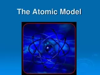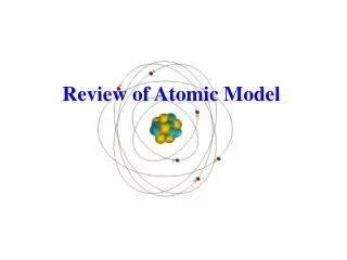
Atomic model
Atomic model. Semi-classical view of atom excitations. Energy. Atom in ground state. Energy. Atom in excited state. MIT 2.71/2.710 Optics 10/20/04 wk7-b-21. Absorption. Spontaneous emission. Stimulated emission. E 2. E 1. Boltzmann’s equation.

Atomic model
E N D
Presentation Transcript
Semi-classical view of atom excitations Energy Atom in ground state Energy Atom in excited state MIT 2.71/2.710 Optics 10/20/04 wk7-b-21
E2 E1 Boltzmann’s equation example: T=3000 K E2-E1=2.0 eV • n1 - the number of electrons of energy E1 • n2 - the number of electrons of energy E2
Einstein’s coefficients Probability of stimulated absorption R1-2 R1-2 = r (n) B1-2 Probability of stimulated and spontaneous emission : R2-1 = r (n) B2-1 + A2-1 assumption: n1 atoms of energy e 1 and n2 atoms of energy e 2 are in thermal equilibrium at temperature T with the radiation of spectral density r (n): n1 R1-2 = n2 R2-1 n1r (n) B1-2 = n2 (r (n) B2-1 + A2-1) E2 E1
According to Boltzman statistics: • r (n) = = Planck’s law B1-2/B2-1 = 1
The probability of spontaneous emission A2-1 /the probability of stimulated emission B2-1r(n ): • Visible photons, energy: 1.6eV – 3.1eV. • kT at 300K ~ 0.025eV. • stimulated emission dominates solely when hn /kT <<1! • (for microwaves: hn <0.0015eV) • The frequency of emission acts to the absorption: • if hn /kT <<1. x~ n2/n1
For lasing action • Active medium • Pumping mechanism • Optical • Electrical discharge • Chemical pumping • Optical resonator Resonator
Carbon Di Oxide LASERPrincipleThe transition between the rotational and vibrationalenergy levels lends to the construction of a molecular gas laser.Nitrogen atoms areraised to the excited state which in turn deliver energy to the CO2 atoms whose energy levels are close to it. Transition takes place between the energy levels of CO2 atoms and the laser beam is emitted.
Applications • Bloodless surgery • Open air communication • Military field
Nd (Neodymium) – YAG (Yttrium Aluminium Garnet) LASERPrincipleCharacteristics Doped Insulator laser refers to yttrium aluminium garnet doped with neodymium. The Nd ion has many energy levels and due to optical pumping these ions are raised to excited levels. During the transition from the metastable state to E1, the laser beam of wavelength 1.064μm is emitted
M1– 100% reflector mirror M2 – partial reflector mirror Laser Rod Flash Tube Resistor Nd (Neodymium) – YAG (Yttrium Aluminium Garnet) LASER Capacitor Power Supply
E3 Non radiative decay E2 E4 Laser 1.064μm E1 Non radiative decay E0 Nd E1, E2, E3 – Energy levels of NdE4 – Meta Stable StateE0 – ground State Energy LevelApplicationsTransmission of signals over large distancesLong haul communication systemEndoscopic applicationsRemaote sensing Energy Level Diagram of Nd– YAG LASER
HOMOJUNCTION SEMICONDUCTOR LASER(Ga-As Laser) Principle • The electron in the conduction band combines with a hole in the valence band and the recombination produces radiant energy. This photon induces another electron in the CB to combine with a hole in the VB and thereby stimulate the emission of another photon.
P- and N-type Semiconductors • In the compound GaAs, each gallium atom has three electrons in its outermost shell of electrons and each arsenic atom has five. When a trace of an impurity element with two outer electrons, such as zinc, is added to the crystal. The result is the shortage of one electron from one of the pairs, causing an imbalance in which there is a “hole” for an electron but there is no electron available. This forms a p-type semiconductor. • When a trace of an impurity element with six outer electrons, such as selenium, is added to a crystal of GaAs, it provides on additional electron which is not needed for the bonding. This electron can be free to move through the crystal. Thus, it provides a mechanism for electrical conductivity. This type is called an n-type semiconductor.
Reverse-biased pn Junction A reverse bias widens the depletion region, but allows minority carriers to move freely with the applied field. Optical Fiber communications, 3rd ed.,G.Keiser,McGrawHill, 2000
Forward-biased pn Junction Lowering the barrier potential with a forward bias allows majority carriers to diffuse across the junction. Optical Fiber communications, 3rd ed.,G.Keiser,McGrawHill, 2000
Applications • Compact & used in fibre optic communications • CD writer • Relieves pain • Laser printers
Excimer LASER • Excited dimer • Short lived molecule formed from one or two species, at least one of which is in an electronically excited state • May not be stable in ground state • Excimer LASER: • Electron pumped LASER • Dimer (excimer)/complex (exciplex) formation • LASER radiation: relaxation from excited state dimer to ground state • Excimer • Function • Chemicals • Characteristic • applications • Organic Dye • Chemicals • Function • Characteristic • applications
Excimer e- + A → A* A* + B → AB* → AB + hν Immediately AB → A + B Two important facts: • The lower state does not exist! • No rotational/vibrational bands • Excimer • Function • Chemicals • Characteristic • applications • Organic Dye • Chemicals • Function • Characteristic • applications
Excimer LASER Energy states of an excimer • Excimer • Function • Chemicals • Characteristic • applications • Organic Dye • Chemicals • Function • Characteristic • applications
Excimer • Excited Dimers • F2, Xe2 ect. • Excited Complexes (Exciplex) • Combination of rare gas atoms and halogen atoms • Ar, Kr, Xe • F, Cl, Br • Excimer • Function • Chemicals • Characteristic • applications • Organic Dye • Chemicals • Function • Characteristic • applications
Excimer LASER • Many wavelength possibilities • Depends upon the excited dimer • Repetition rate from 0.05 Hz to 20 kHz • High power: • several 10-200 W • Excimer • Function • Chemicals • Characteristic • applications • Organic Dye • Chemicals • Function • Characteristic • applications
Excimer LASER • Micromaching • Ink jet cartidges (drilling the nozzles) • Radiation for changing the structure and properties of materials • Active matrix LCD monitors • Fiber bragg gratings • High temperature superconducting films • “Short wavelength light bulb” in optical litography • Computer chips • Excimer • Function • Chemicals • Characteristic • applications • Organic Dye • Chemicals • Function • Characteristic • applications
S S S N N N N N S S 1. Introduction The Free Electron Laser (FEL) consists of a relativistic beam of electrons (v≈c) moving through a spatially periodic magnetic field (wiggler). Relativistic electron beam EM radiation llw /g2 << lw Magnetostatic “wiggler” field (wavelength lw) • Principal attraction of the FEL is tunability : • - FELs currently produce coherent light from microwaves • through visible to UV • X-ray production via Self- Amplified Spontaneous Emission (SASE) (LCLS – 1.5Å)
Principle Two beams (object beam and reference beam) are superimposed on a holographic plate to form an image called a hologram.
Principle A beam of light (reading beam) having the same wavelength as that of the reference beam used for constructing the hologram, is made to fall over the hologram, which in turn gives rise to a 3-D image in the field of view.
Review of Semiconductor Physics a) Energy level diagrams showing the excitation of an electron from the valence band to the conduction band. The resultant free electron can freely move under the application of electric field. b) Equal electron & hole concentrations in an intrinsic semiconductor created by the thermal excitation of electrons across the band gap Optical Fiber communications, 3rd ed.,G.Keiser,McGrawHill, 2000
n-Type Semiconductor • Donor level in an n-type semiconductor. • The ionization of donor impurities creates an increased electron concentration distribution. Optical Fiber communications, 3rd ed.,G.Keiser,McGrawHill, 2000
p-Type Semiconductor • Acceptor level in an p-type semiconductor. • The ionization of acceptor impurities creates an increased hole concentration distribution Optical Fiber communications, 3rd ed.,G.Keiser,McGrawHill, 2000
The pn Junction Electron diffusion across a pn junction creates a barrier potential (electric field) in the depletion region. Optical Fiber communications, 3rd ed.,G.Keiser,McGrawHill, 2000