Download
1 / 70
700 likes | 889 Vues
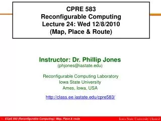
CPRE 583 Reconfigurable Computing Lecture 24: Wed 12/8/2010 (Map, Place & Route). Instructor: Dr. Phillip Jones (phjones@iastate.edu) Reconfigurable Computing Laboratory Iowa State University Ames, Iowa, USA. http://class.ee.iastate.edu/cpre583/. Announcements/Reminders.

E N D
CPRE 583Reconfigurable ComputingLecture 24: Wed 12/8/2010(Map, Place & Route) Instructor: Dr. Phillip Jones (phjones@iastate.edu) Reconfigurable Computing Laboratory Iowa State University Ames, Iowa, USA http://class.ee.iastate.edu/cpre583/
Announcements/Reminders • HW3: finishing up (hope to release this evening) will be due Fri12/17 midnight. • Two lectures left • Fri 12/3: Synthesis and Map • Wed 12/8: Place and Route • Two class sessions for Project Presentations • Fri 12/10 • Wed 12/15 (9 – 10:30 am) • Take home final given on Wed 12/15 due 12/17 5pm
Initial Project Proposal Slides (5-10 slides) • Project team list: Name, Responsibility (who is project leader) • Team size: 3-4 (5 case-by-case) • Project idea • Motivation (why is this interesting, useful) • What will be the end result • High-level picture of final product • High-level Plan • Break project into mile stones • Provide initial schedule: I would initially schedule aggressively to have project complete by Thanksgiving. Issues will pop up to cause the schedule to slip. • System block diagrams • High-level algorithms (if any) • Concerns • Implementation • Conceptual • Research papers related to you project idea
Projects Ideas: Relevant conferences • Micro • Super Computing • HPCA • IPDPS • FPL • FPT • FCCM • FPGA • DAC • ICCAD • Reconfig • RTSS • RTAS • ISCA
Initial Project Proposal Slides (5-10 slides) • Project team list: Name, Responsibility (who is project leader) • Project idea • Motivation (why is this interesting, useful) • What will be the end result • High-level picture of final product • High-level Plan • Break project into mile stones • Provide initial schedule: I would initially schedule aggressively to have project complete by Thanksgiving. Issues will pop up to cause the schedule to slip. • System block diagrams • High-level algorithms (if any) • Concerns • Implementation • Conceptual • Research papers related to you project idea
Final Project Presentation (12-15 slides) • Project team list: Name, Responsibility (who is project leader) • Project idea • Motivation (why is this interesting, useful) • High-level picture of final product • Implementation • System block diagrams • High-level algorithms (if any) • Lessons learned • Design issue realizations • Implementation issues • Research papers related to you project idea
Weekly Project Updates • The current state of your project write up • Even in the early stages of the project you should be able to write a rough draft of the Introduction and Motivation section • The current state of your Final Presentation • Your Initial Project proposal presentation (Due Fri 10/22). Should make for a starting point for you Final presentation • What things are work & not working • What roadblocks are you running into
Projects: Target Timeline • Teams Formed and Idea: Mon 10/11 • Project idea in Power Point 3-5 slides • Motivation (why is this interesting, useful) • What will be the end result • High-level picture of final product • Project team list: Name, Responsibility • High-level Plan/Proposal: Fri 10/22 • Power Point 5-10 slides • System block diagrams • High-level algorithms (if any) • Concerns • Implementation • Conceptual • Related research papers (if any)
Projects: Target Timeline • Work on projects: 10/22 - 12/8 • Weekly update reports • More information on updates will be given • Presentations: Last Wed/Fri of class • Present / Demo what is done at this point • 25-30 minutes (depends on number of projects) • Final write up and Software/Hardware turned in (Fri: 12/17).
Project Grading Breakdown • 50% Final Project Demo • 30% Final Project Report • 30% of your project report grade will come from your 5-6 project updates. Friday’s midnight • 20% Final Project Presentation
Outline • Mapping a synthesized circuit to FPGA components • Placing components on the FPGA • Routing: connecting components
Applications on FPGA: Low-level • Implement circuit in VHDL (Verilog) • Simulate compiled VHDL • Synthesis VHDL into a device independent format • Map device independent format to device specific resources • Check that device has enough resources for the design • Place resources onto physical device locations • Route (connect) resources together • Completely routed • Circuit meets specified performance • Download configuration file (bit-steam) to the FPGA
Applications on FPGA: Low-level Implement Simulate Synthesize Map Place Route Download
(Technology) Map • Translate device independent net list to device specific resources
(Technology) Map • Translate device independent net list to device specific resources
(Technology) Map • Translate device independent net list to device specific resources
(Technology) Map • Translate device independent net list to device specific resources
Applications on FPGA: Low-level Implement Simulate Synthesize Map Place Route Download
Place • Bind each mapped resource to a physical device location • User Guided Layout (Chapter 16:Reconfigurable Computing) • General Purpose (Chapter 14:Reconfigurable Computing) • Simulated Annealing • Partition-based • Structured Guided (Chapter 15:Reconfigurable Computing) • Data Path based • Heuristics used • No efficient means for finding an optimal solution
Place (High-level) Netlist from technology mapping in A in B in C RAM E DFF F LUT D DFF G clk out
Place (High-level) Netlist from technology mapping FPGA physical layout I/O I/O I/O I/O in A in B in C I/O BRAM I/O LUT LUT RAM E I/O I/O DFF F LUT D LUT I/O I/O LUT BRAM I/O LUT I/O LUT DFF G I/O I/O clk LUT I/O LUT I/O out I/O I/O I/O I/O
Place (High-level) Netlist from technology mapping FPGA physical layout clk in C out I/O in A in B in C In A E I/O LUT G D F RAM E In B I/O DFF F LUT D LUT I/O I/O LUT BRAM I/O LUT I/O LUT DFF G I/O I/O clk LUT I/O LUT I/O out I/O I/O I/O I/O
Place • User Guided Layout (Chapter 16:Reconfigurable Computing • General Purpose (Chapter 14:Reconfigurable Computing) • Simulated Annealing • Partition-based • Structured Guided (Chapter 15:Reconfigurable Computing) • Data Path based
Place (User-Guided) • User provide information about applications structure to help guide placement • Can help remove critical paths • Can greatly reduce amount of time for routing • Several methods to guide placement • Fixed region • Floating region • Exact location • Relative location
Place (User-Guided): Examples Part of Map Netlist DFF F LUT D DFF G FPGA Fixed region
Place (User-Guided): Examples Part of Map Netlist DFF F SDRAM LUT D DFF G FPGA Fixed region
Place (User-Guided): Examples Floating region FPGA Softcore Processor
Place (User-Guided): Examples Part of Map Netlist DFF F LUT D DFF G FPGA Exact Location LUT BRAM LUT LUT LUT LUT LUT LUT LUT BRAM LUT LUT LUT LUT LUT LUT LUT LUT
Place (User-Guided): Examples Part of Map Netlist DFF F LUT D DFF G FPGA Exact Location LUT BRAM LUT LUT G LUT D F LUT LUT LUT BRAM LUT LUT LUT LUT LUT LUT LUT LUT
Place (User-Guided): Examples Part of Map Netlist G DFF F D F LUT D DFF G FPGA Relative Location LUT BRAM LUT LUT LUT LUT LUT LUT LUT BRAM LUT LUT LUT LUT LUT LUT LUT LUT
Place (User-Guided): Examples Part of Map Netlist G DFF F D F LUT D DFF G FPGA Relative Location LUT BRAM LUT LUT LUT LUT LUT LUT LUT BRAM LUT LUT LUT LUT LUT LUT LUT LUT
Place (User-Guided): Examples Part of Map Netlist G DFF F D F LUT D DFF G FPGA Relative Location LUT BRAM LUT LUT LUT LUT LUT LUT LUT BRAM LUT LUT LUT LUT LUT LUT LUT LUT
Place • User Guided Layout (Chapter 16:Reconfigurable Computing • General Purpose (Chapter 14:Reconfigurable Computing) • Simulated Annealing • Partition-based • Structured Guided (Chapter 15:Reconfigurable Computing) • Data Path based
Place (General Purpose) • Characteristics: • Places resources without any knowledge of high level structure • Guided primarily by local connections between resources • Drawback: Does not take explicit advantage of applications structure • Advantage: Typically can be used to place any arbitrary circuit
Place (General Purpose) • Preprocess Map Netlist using Clustering • Group netlist components that have local conductivity into a single logic block • Clustering helps to reduce the number of objects a placement algorithm has to explicitly place.
Place (General Purpose) • Placement using simulated annealing • Based on the physical process of annealing used to create metal alloys
Place (General Purpose) • Simulated annealing basic algorithm • Placement_cur = Inital_Placement; • T = Initial_Temperature; • While (not exit criteria 1) • While (not exit criteria 2) • Placement_new = Modify_placement(Placement_cur) • ∆ Cost = Cost(Placement_new) – Cost(Placement_cur) • r = random (0,1); • If r < e^(-∆Cost / T), Then Placement_cur = Placement_new • End loop • T = UpdateTemp(T); • End loop
Place (General Purpose) G D F • Simulated annealing: Illustration FPGA LUT BRAM LUT X LUT LUT A Z LUT BRAM LUT B LUT LUT LUT LUT LUT LUT
Place (General Purpose) LUT F • Simulated annealing: Illustration FPGA LUT BRAM LUT LUT LUT LUT G LUT Z LUT BRAM X B LUT A LUT LUT LUT D
Place (General Purpose) G D F • Simulated annealing: Illustration FPGA LUT BRAM LUT X LUT LUT A Z LUT BRAM LUT B LUT LUT LUT LUT LUT LUT
Place (General Purpose) G D F • Simulated annealing: Illustration FPGA LUT BRAM LUT X LUT LUT LUT Z A BRAM LUT B LUT LUT LUT LUT LUT LUT
Place (General Purpose) G D F • Simulated annealing: Illustration FPGA LUT BRAM LUT LUT LUT X LUT Z A BRAM LUT B LUT LUT LUT LUT LUT LUT
Place • User Guided Layout (Chapter 16:Reconfigurable Computing • General Purpose (Chapter 14:Reconfigurable Computing) • Simulated Annealing • Partition-based • Structured Guided (Chapter 15:Reconfigurable Computing) • Data Path based
Place (Structured-based) • Leverage structure of the application • Algorithms my work well for a give structure, but will likely give unacceptable results for an design with little regular structure.
Applications on FPGA: Low-level Implement Simulate Synthesize Map Place Route Download
Route • Connect placed resources together • Two requirements • Design must be completely routed • Routed design meets timing requirements • Widely used algorithm “PathFinder” • PathFinder (FPGA’95) • McMurchie and Ebeling • Reconfigurable Computing (Chapter 17) • Scott Hauch, Andre Dehon (2008)
Route (PathFinder) • PathFinder: A Negotiation-Based Performance-Driven Router for FPGAs (FPGA’95) • Basic PathFinder algorithm • Based closely on Djikstra’s shortest path • Weights are assigned to nodes instead of edges
Route (PathFinder): Example • G = (V,E) • Vertices V: set of nodes (wires) • Edges E: set of switches used to connect wires • Cost of using a wire: c_n = (b_n + h_n) * p_n S1 S2 S3 2 3 1 4 3 1 1 A B C 1 1 3 4 1 3 2 D1 D2 D3