Design Rules for Metal-Semiconductor Contacts in EE143 by Ali Javey
This document outlines essential design rules for absolute-value layouts in the EE143 course, specifically addressing metal-semiconductor contact configurations. Key specifications include minimum contact hole sizes, defined spacing between metal lines, overlap criteria for contacts, and considerations for gate oxide areas. Emphasis is placed on avoiding shorting and ensuring consistency in topography. Guidelines for dealing with CVD SiO2 deposition and potential etching problems are also discussed, ensuring optimal performance in semiconductor applications.

Design Rules for Metal-Semiconductor Contacts in EE143 by Ali Javey
E N D
Presentation Transcript
Section 10: Layout EE143 –Ali Javey
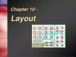
Layout Design Rules (1) Absolute-Value Design Rules * Use absolute distances (2) -based Design Rules EE143 –Ali Javey 2
Metal-Si Contact Hole (same rule for Metal-poly) Min. contact hole = 2 x 2 Min contact hole to diffusion layer distance = Al SiO2 SiO2 n+ n+ p-sub p-sub EE143 –Ali Javey
Metal Lines Line 1 Min width = 2 Min. metal-metal spacing = 3 Line 2 [Rationale] metal runs on rough topography 3 spacing to ensure no shorting between the 2 lines. EE143 –Ali Javey
M1-Contact Overlap Min overlap of contact hole = Etching problem CVD SiO2 deposition. problem in narrow gap SiO2 • Si EE143 –Ali Javey
Poly-Si Gate Min gate-overlap of field oxide = Avoid n+ channel formation during S/D Implant n+ n+ n+ ideal With overlay error EE143 –Ali Javey
Gate contacting Comment: Al to poly contact should not be directly on top of gate oxide area Al Poly gate Gate oxide Si Al Al ~400OC Al spike Poly Poly SiO2 SiO2 Si Si EE143 –Ali Javey