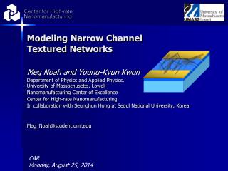
Modeling Narrow Channel Textured Networks
410 likes | 539 Vues
This study presents a comprehensive modeling approach to evaluate the electronic properties of anisotropic nanotube networks, essential for advancing high-performance nanoscale transistors. Our method employs Monte Carlo simulations and Kirchhoff's laws to analyze channels within a random network structure, accounting for mixed chirality nanotubes. We report significant findings indicating that reduced channel width enhances conductivity and mobility compared to traditional devices. The model aids in predicting the performance of environmental sensors and provides insights into optimal manufacturing parameters for successful mass production.

Modeling Narrow Channel Textured Networks
E N D
Presentation Transcript
Modeling Narrow Channel Textured Networks Meg Noah and Young-Kyun Kwon Department of Physics and Applied Physics, University of Massachusetts, Lowell Nanomanufacturing Center of Excellence Center for High-rate Nanomanufacturing In collaboration with Seunghun Hong at Seoul National University, Korea Meg_Noah@student.uml.edu
Nanotube Properties Not Connected Semiconductor Metallic Classification of Channels Metallic Semiconductors
Channel Properties Not Conducting Metallic Semiconductor Motivation • Traditional isotropic models present manufacturing showstoppers! • Modeling community has not yet produced statistical simulations of anisotropic nanotube networks. • Affordable solutions of nanotubes are mixed chiralty, and when the density is too high, the channels are conductors. • Even when the channel is semiconducting, the on-off ratio is poor due to the presence of metallic NT. • Reported values of short channel width randomly-oriented SWNT networks ~ w1.53 pose manufacturing problems. Behnam, et al APL 2006
Objectives • Model electronic properties of anisotropic nanotube networks. • Determine the feasibility of using mixed chirality nanotubes. • Model ensembles of nanotube networks from a statistical characterization of a nanotube mixture. • Extend NTFET model to sensor model.
Methodology • Represent the device as a 2D random network of nanotubes of specified length, Ls, and conductivity, G, dispersed in a channel of length, L, and width, W. • Represent the system as a network of nodes and resistors • [Reduce the grid using Kirchhoff’s Laws] • Compute electronic properties • Monte Carlo simulations • Model the distribution functions of each class (eg metallic, semiconducting, defective) as a function of CNT density. • An analytical expression derived from model output provides a fast estimation of probability of success for a give manufacturing parameter set.
Channel Properties Not Conducting Metallic Semiconductor Overview • We present a model of nanotube network channels and its application to high-performance nanoscale transistors. • The model predicts electronic properties of single channels, and statistical metrics of ensembles of channels.
Take-Home Message Both experimental and simulation results show that the conductivity and mobility of textured network devices increased with reduced channel width, unlike random network-based or conventional silicon-based devices. Our model answers many ‘what if’ questions: Do textured networks offer advantages over traditional percolations as environmental sensors? Can the properties of a network in an environment be predicted if the NT properties are statistically known? What manufacturing parameters would result in feasible mass production of such an environmental sensor? What strategies, including logical combinations of sensors, work for optimizing selectivity? Sensitivity? Is it better to have optimal semiconducting properties, or better to have more NT even if the channel is more metallic?
Publications Journal Articles Hahm, Noah, Kwon, Jung, Diameter Selective Growth of Vertically Aligned Single Walled Carbon Nanotubes by Ethanol Flow Control, Nanotech 2008 Vol. 1 Lee, Noah, Park, Seong, Kwon, and Hong, “Textured” Network Devices: Overcoming Fundamental Limitations of Nanotube/Nanowire Network-Based Devices, Small (2009) Lee, Baik, Noah, Kwon, Lee, and Hong, Nanowire and Nanotube transistors for lab-on-a-chip applications, Lab on a Chip, Issue 16 (2009) APS Presentations Noah and Kwon, Toward 100% Semiconducting Devices From Mixed Chirality Nanotube Networks (2007) Lee, Im, Lee, Myung, Kang, and Hong, Large-Scale Array of Pristine Carbon Nanotube Transistors (2007) Noah and Kwon, Modeling Narrow Channel Textured Networks (2008) Lee, Hong, Noah, Kwon, Park, and Seong, Fabrication of Long Channel Carbon Nanotube Network Transistor Arrays (2008) Park, Lee, Lee, Hong, Kwon, Noah, Park, Seong, Structural Control of Carbon Nanotube Networks for High-Performance Devices (2010) CHN Poster Papers
Traditional Percolating Systems • Derivation of percolation threshold, the critical density of sticksof a given length to percolate. Pike and Seager PRB 1974 • Define critical stick length LS for given density of sticks. Derivation of percolation critical exponents. ‘Conductivity’ exponent (LS / LTH )2shown to be t=1.24±0.03. Define anisotropy metric. Balberg, Binenbaum, & Anderson PRL 1983 • Conductivity is a power of the channel length. ~ LC.Relations of ISD to LS for isotropic systems.Pimparker, Guo, Alam NCN at NanoHUB.org 2006 • Conductivity is a power of the average NT bundle length. ~ LSa Hecht, Hu, Grüner APL 2006 • Conductivity is a power of the channel width for NT networks. ~ LW. Behnam, et al APL 2006
SNU New Process, Anisotropic Network 1. Pattern an Alignment Key onto a substrate. 2. Assemble the CNT onto the substrate. 3. Pattern the electrodes onto the CNT channels. 4. Deposit a SiO2 film over the electrodes, CNT channel, and substrate. 5. Pattern on the Gate after selective burning Back-Gate.
Probability Distribution of each device class (metallic, not connected, semiconductor, success, false alarm, missed detection) IV Characteristics Equivalent Circuits Channel Dimensions Property Distribution NT Network Sensor Model Environment Success Criteria Number of Trials Bias Voltage Nanotube Properties WinSpice Length/Type Distribution Nanotube Conductivity Contact Resistances Measured and Modeled Environmental Sensitivity Functionalized Variations Model Description NT Network Model
Model Description Read User Inputs Populate Channel Loop for nTrials Find NT-Electrode Intersections Loop for nEnvironments Find NT-NT Crossings Model Single Nanotube Network Channel Table of Nodes/Resistors For Equivalent Circuit Assign Classification Tabulate Results Compute IV Curve Probability Distributions For Different Classes IV Curves
Semiconducting Nanotubes • G=Cm(Vg0-Vg)/L • C ~ 60 aF • m ranges from 1000 to 20000 cm2/V s • CNT Contact Electrode • Model Value = 50 kΩ • McEuen, P. and Ji-Yong Park, 'Electron Transport in Single-Walled Carbon Nanotubes', MRS BUlletin, April 2004 • Burke, PJ 'An RF Circuit Model for Carbon Nanotubes' IEEE-NANO 2002 • Ilani, et. al, 'Measurement of the quantum capacitance of interacting electrons in carbon nanotubes', Nature Physics, Vol 2, Oct. 2006 • Contact Points at CNT Junctions.1 to .3 Go (43 to 129 kΩ) • Model Value = 40 kΩ • Yoon, et. al., Physical Review Letters Vol. 86, No. 4, 2001 Predicting I-V Curves for Ensemble • Metallic SWNT • Model Value = 4 kΩ/mm • McEuen, P. and Ji-Yong Park, 'Electron Transport in Single-Walled Carbon Nanotubes', MRS Bulletin, April 2004
Database – NT Length, LS • Input length allowed to vary up to +/- input standard deviation value from a Gaussian random number. Most of our results were LS • 2) Measured Lengths for 0.1 mg/mL o-dichlorobenzene SWNT suspensions
Database Nanotube Molecular Wires as Chemical Sensors Jing Kong, et al., Science 287, 622 (2000) Yoon, Mazzoni, Choi, Ihm, Louie PRL, 2001
Manufacturing Success Failure in Manufacturing Not Connected ISD < 10-10 A SemiconductorIOFF < 10-10 AISD > 10-8 A Metallic 10-8 A > ISD Classification as a Transistor Nanotube Properties Metallic Semiconductors
Isotropic Channels Anisotropy ~ 1 Anisotropic Channels Anisotropy≠1 Classification as a Texture
Channel Properties Not Conducting Semiconductor Metallic Increasing Channel Length, L
Channel Properties Not Conducting Semiconductor Metallic Increasing Channel Width, W
Channel Properties Not Conducting Semiconductor Metallic Increasing Fraction of Metallic NT
Analytical Expression r0 = Density at which 50% of devices are connected = f(L,W) μ = Asymmetry factor, value fit as 0.0404 γ = Slope factor = 0.2848 β = Scaling factor = 25.9704 f = fraction of nanotubes that are metallic Note: Values for dimensions greater than nanotube length.
Validation: Scaling with NT Length General Result: Balberg, Binenbaum, Anderson PRL 1983 ~ LS2.48 Hecht, APL (89) 2006 ~ LSa 0 < a < 2 Our model Note: When the tubes in the network approach 20–30 microns, the resistance along the tube itself becomes comparable to the resistance of the junction
Validation: Scaling Channel Length Pimparkar, Guo, Alam NCN NanoHUB, 2006 Our model.
Long Channel Low Density of CNT Validation: I-V Curves of Individual Devices Modeled Measured
Validation: I-V Curves of Individual Devices Long ChannelHigh Density of CNT Modeled Measured
Validation: Probability of Success Channel: 20 mm x 3 mm Modeled Measured
Validation: Probability of Success Channel: 20 mm x 16 mm Modeled Measured
Validation: Ensemble Conductivity Modeled Measured
Validation: Ensemble Mobility Modeled Measured
Modeling NT Network Sensors • Performance Metrics • sensitivity • stability • selectivity • Classification • Success • Missed Detection • False Alarm (ID) • False Alarm (Quantity) • Sensor Suites • Evaluating Selective Strategies • Two channels with different responses to same gas used to logically • Voting • Dynamic Range and Sensitivity • Improved sampling • Dynamic Flow
Failure in Sensing Missed Detection False Alarm (Identify) Sensitivity, Stability, Response Time Positive Detection Success in Sensing Classification as a Sensor vs
Sensor Model Results sA=4.0 sE=6.4 Scm-1 @ Vg=-0.75 V 4 micron x 1 micron, 1/3 metallic NT, ‘saturated’
Sensor Model Results sA=11.7 sE=17 Scm-1 4 micron x 1 micron, 1/3 metallic NT, ‘saturated’
Sensor Model Results sA=94.8 sE=105.3 Scm-1 4 micron x 1 micron, 1/3 metallic NT, ‘saturated’
Concept for an Accelerometerfor microgravity • Structural relaxation of a (5,5) crossed SWNT junction with a 15 nN contact force. • Contact distance (.25 nm) reduced by 20% from the van der Waals distance. • Center-to-center distance is 0.74 nm. (Free space distance would be about 1.01 nm) • Tried a 4x1 (very anisotropic) channel:20 junction = 2.94 µA at VG=-6V40 junction = 2.87 µA
We have developed a model for estimating the probability of successful and defective semiconductors resulting from a set of manufacturing parameters. For example, over 90% of an ensemble of 40x2 µm nanotube networks, of 1/3 metallic content and 4 NT/µm2, will have semiconductor properties. An analytical function was fit to model output. We can predict the I-VCurves of the nanotube networks by finding an equivalent circuit of resistors and nodes. Summary
Our results: Explain why measurements of textured networks show improved conductivity with narrow channels. Show that traditional percolation models are insufficient for textured networks. Characterize nanotube network ensembles. Model the network I-V, s, m in different environments. Conclusions
Expand database of nanotube parameters Dispersions with bundling Substrate dependence Environmental factors Model SWNT transmission Different nanotubes – Nickel or Gold Model ensemble statistics ofI-V curves and values quantifying production parameters in terms of mobility, dynamic range, etc. Connection to percolation models Verification and validation with experimental data Future Work
Defect Analysis Additional V&V Model nanotube network performance as a sensor Functionalization forselectivity:Ara h 1 molecule Future Work Maleki, Soheila J., et. al, The Journal of Immunology, 2000