PS/2 mouse control using EOG/EMG signals
360 likes | 622 Vues
PS/2 mouse control using EOG/EMG signals. Group #9 Vikas Gupta Nick Chang. Overview. PS/2 mouse controlled with eyes Original Design Specification Deviations Functionality Tests Challenges Improvements Conclusion. Objective. Many people unable to use a mouse

PS/2 mouse control using EOG/EMG signals
E N D
Presentation Transcript
PS/2 mouse control using EOG/EMG signals Group #9 Vikas Gupta Nick Chang
Overview • PS/2 mouse controlled with eyes • Original Design • Specification Deviations • Functionality Tests • Challenges • Improvements • Conclusion
Objective • Many people unable to use a mouse • Create a device which allows people to control mouse cursor with eye movements • Goals • Obtain useable logic signals from eyes • Convert signals into instructions the computer can understand • Personal Interests • Implement something cool!
Original Design Signal Filtering and Amplification EOG electrodes wires Computer Field Programmable Gate Array PS/2 male-male connector
Original Design Signal Filtering and Amplification EOG electrodes
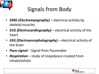
Obtaining The Biosignal • 0.4 – 1 mV potential between Cornea and Retina • Use electrodes to measure potential
Electrode Placement • Red electrodes capture lateral eye movement • Blue electrodes capture vertical eye movement • Black electrode is common ground
Amplification, Filtration, Isolation Non- inverting Amp Rectifier Up 4th Order Filter Input Buffer Diff. Amp Inverting Amp Summer Circuit Down Rectifier Inverting Amp Ground Non- inverting Amp Ground Rectifier Right 4th Order Filter Input Buffer Diff. Amp Inverting Amp Summer Circuit Left Rectifier Inverting Amp Output
Amplification, Filtration, Isolation Non- inverting Amp Rectifier Up 4th Order Filter Input Buffer Diff. Amp Inverting Amp Summer Circuit Down Rectifier Inverting Amp Ground Non- inverting Amp Rectifier Right 4th Order Filter Input Buffer Diff. Amp Inverting Amp Summer Circuit Left Rectifier Inverting Amp Output
Amplification, Filtration, Isolation Non- inverting Amp Rectifier Up 4th Order Filter Input Buffer Diff. Amp Inverting Amp Summer Circuit Down Rectifier Inverting Amp Ground Non- inverting Amp Rectifier Right 4th Order Filter Input Buffer Diff. Amp Inverting Amp Summer Circuit Left Rectifier Inverting Amp Output
Amplification, Filtration, Isolation Non- inverting Amp Rectifier Up 4th Order Filter Input Buffer Diff. Amp Inverting Amp Summer Circuit Down Rectifier Inverting Amp Ground Non- inverting Amp Rectifier Right 4th Order Filter Input Buffer Diff. Amp Inverting Amp Summer Circuit Left Rectifier Inverting Amp Output
Amplification, Filtration, Isolation Non- inverting Amp Rectifier Up 4th Order Filter Input Buffer Diff. Amp Inverting Amp Summer Circuit Down Rectifier Inverting Amp Ground Non- inverting Amp Rectifier Right 4th Order Filter Input Buffer Diff. Amp Inverting Amp Summer Circuit Left Rectifier Inverting Amp Output
Amplification, Filtration, Isolation Non- inverting Amp Rectifier Up 4th Order Filter Input Buffer Diff. Amp Inverting Amp Summer Circuit Down Rectifier Inverting Amp Ground Non- inverting Amp Rectifier Right 4th Order Filter Input Buffer Diff. Amp Inverting Amp Summer Circuit Left Rectifier Inverting Amp Output
Amplification, Filtration, Isolation Non- inverting Amp Rectifier Up 4th Order Filter Input Buffer Diff. Amp Inverting Amp Summer Circuit Down Rectifier Inverting Amp Ground Non- inverting Amp Rectifier Right 4th Order Filter Input Buffer Diff. Amp Inverting Amp Summer Circuit Left Rectifier Inverting Amp Output
Amplification, Filtration, Isolation Non- inverting Amp Rectifier Up 4th Order Filter Input Buffer Diff. Amp Inverting Amp Summer Circuit Down Rectifier Inverting Amp Ground Non- inverting Amp Rectifier Right 4th Order Filter Input Buffer Diff. Amp Inverting Amp Summer Circuit Left Rectifier Inverting Amp Output
Original Design Field Programmable Gate Array Computer • 2 main components: • Master State machine • Controls when the mouse should send/receive • Sensor Decision Logic • Convert inputs into mouse words
Original Design Original Design • Block Diagram of FPGA components from our Design Review: Mouse Word (3 bytes) Left Decision Logic State Machine Right PS/2 Interface Down Up Step Down Counter 15 kHz PS/2 Oscillator
Project Build – Signal Circuitry • Input Buffer • Unity gain • 3.3/3.3 = 1
Project Build – Signal Circuitry • Difference Amplifier • R1 = R2, R3 = R4 • Av = R4 / R2 • Av = 33/3.3 = 10V/V
Project Build – Signal Circuitry • 4th Order Butterworth Filter • Maximally flat passband • Cascade two 2nd order filters • H(s) = Avo/B(s) • B(s) = s2+1.414s+1 • Avo = 3 – 1.414 = 1.586 • Total gain = (1.586)*(1.586) = 2.515 V/V • 1.586 = R1’/R1 • R1 = 10K, R1’ = 5.86K • Want Fo ~33 Hz • 33 = (2*pi*R*C)-1 • Let R = 10K, C = 0.47uF
Project Build – Signal Circuitry • Inverting Amplifier • Avo = -R2/R1 • Up/Down • Avo = -82/1.2 = 68.3 V/V • Left/Right • Avo = -68/1.2 = 56.6 V/V
Project Build – Signal Circuitry • Summer Circuit • Can add +/- 12V to input signal • Unity gain • 10/10 = 1 V/V
Project Build – Signal Circuitry • Inverting / Non Inverting Amplifier & Rectifier • Inverting Gain Non Inverting Gain Avo = 33/3.3 = 10 V/V Avo = 1 + 33/3.3 = 11V/V
Project Build – FPGA mouse • XSA-100 Prototyping Board • Conveniently comes with a PS/2 port • 555 IC Timer (x2) • Generation of arbitrary frequency clocks (a function of external R and C elements) • 30 kHz clock – PS/2 signal clock • slow clock – large state machine
Project Build – FPGA mouse Input from signal circuitry Mouse Word Generator 8-bit Shift Register (Command Word) Onboard Display Send/Receive State Machine Master State Machine Seven Segment Decoder 30 kHz 555 Clk PS/2 Signals to Computer ~150 Hz 555 Clk
Project Build – FPGA mouse Reset If Reset = ‘1’ Init NOT byte_received Clk = ‘1’ Listen Reset Byte_received AND command_word != ‘xF4’ Enable_sendbyte = ‘1’ psClk = 0->1, psData = ‘0’ (Request to Send state) Byte_received AND command_word = ‘xF4’ Send byte_received = ‘1’ Setup Response States Recieve Send Mouse Words Ready Finished
Functional Tests • Independent component tests were feasible with our design • FPGA mouse – switches/LEDs/Logic Analyzer • Signal circuitry – LEDs/Oscilloscope
Challenges – Signal Circuitry • Placement of Electrodes • Slight changes create affect dc baseline • Electrodes too large • Reliability of Signal • Looking “left” had an affect on “down”
Challenges - FPGA • PS/2 protocol occurs at a frequency of 15kHz • Solution: 555 timer • Minor Detail – Major Hurdle! • PS/2 specification website • Large Number of States • A single byte transfer takes 22 states • Strict Timing Requirements
Improvements • Mouse button emulation • Implemented in FPGA, but not in signal circuitry • Blinking • Variable Amplifier Gain • DC Drift • PCB Implementation
Conclusion • It worked! • 8 direction mouse movement • Functionality was as expected • Questions?