Comprehensive Design of Clock and Control Systems for EuXFEL: MTCA.4 Architecture Overview
This document presents the design and development of clock and control (CC) systems for the European X-ray Free Electron Laser (EuXFEL). It highlights the utilization of MTCA.4 architecture and FPGA technology in creating a scalable, flexible DAQ system capable of synchronizing with high-performance detectors. The report discusses the hardware and firmware configurations, supporting various communication protocols, and ensuring extendibility for future upgrades. Various technical specifications and integration strategies are detailed for improved performance in particle physics experiments.

Comprehensive Design of Clock and Control Systems for EuXFEL: MTCA.4 Architecture Overview
E N D
Presentation Transcript
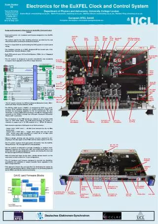
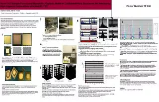
40-pin DIL BREAK-OUT HEADER (incl. 4x diff. pairs 2V5 LVDS ) 3 6x POWER 2x GND pins 3x LEDs 6x FUSES 3 8 24 8 22 16 32 8 7 4 6 16 2 8 4 8 2 7 2 12x LEDs SHIFT REG. 3 VME BASE ADDRESS A<31-24> FPGA & PROM 3 Xilinx Spartan3e XC3S1600E-5FGG400C 3 Buffers SW SW SW SW SW SW VME J2 NIM ECL CLKIN0 CLKIN1 2 2 MPX PLL CLKIN select IN0 NIM TTL CLK Master DELAY 8 8 IN2 20x LEMO-00 4 4 VME J1 40/80MHz select Buffers IN4 4x Slave DELAYS 4 IN6 :2 NIM ECL CLKOUT0 CLKOUT1 2 2 2x LEDs X-TAL 80.15733MHz All POWER Monitor OUT0 NIM TTL 8 8 Data 4Mbx18 SRAM Address OUT2 7 OUT4 +5V +3V3 +2V5 +1V8 +1V2 -5V -2V OUT6 16-pin AUX. CONNECTOR 16 ( incl. 2x diff. pairs 2V5 LVDS ) 6x DC-DC MOD. RECORD J-TAG FUSES USB SHIFT REG. HEX SELECT SERIAL NO. EXT. +5V IN USB MCU MP-UCL, 18 August 2011 Red LED –FPGA Prog. Prog. FPGA Switch GSI 18x4Mb SRAM Ext. 5V/3A Conn. Xilinx PROM Spartan3E FPGA VME Base Address A<31-28> A<27-24> Clock MUX/PLL VME J1 VME J2 80.15733 MHz XTAL Osc. Red LED 3x Supply OK Blue LED 4x Supply OK Clk+4 Delay Lines 7x Supply Monitor Set Serial No. SER<7-4> SER<3-0> 40-pin DIL HEADER DIL JTAG for USB MCU Set Mod. Record MR<7-4> MR<3-0> USB Reset Switch SIL JTAG for FPGA IN<7-0> TTL/NIM Sel. CLK-OUT<1-0> ECL/NIM Sel. OUT<7-0> TTL/NIM Sel. CLK-IN<1-0> ECL/NIM Sel. Ext. +5V / 3A Power Conn. VME J2 VME J1 40-pin DIL HEADER USB MCU JTAG Prog. MODE Hex Switch. Programm. Reset Switch DATA-IN<7-0> 8x LEMOs 00 DATA-OUT<7-0> 8x LEMOs 00 3x STATUS LEDs ( Programmable ) 3x4 LEDs ( Programm. ) Global Reset Switch ( FPGA, MCU ) CLK-IN<1-0> 2x LEMOs 00 CLK-OUT<1-0> 2x LEMOs 00 AUX. DIL 16x I/Os FPGA JTAG 4-pin USB Deutsches Elektronen-Synchrotron Electronics for the EuXFEL Clock and Control System Poster Number 104 Topical Workshop on Electronics for Particle Physics ( TWEPP-2011 ) Vienna, Austria 26 to 30 Sept. 2011 Department of Physics and Astronomy, University College LondonErdem Motuk <emotuk@hep.ucl.ac.uk>, MartinPostranecky <mp@hep.ucl.ac.uk>, Matthew Warren <warren@hep.ucl.ac.uk>, Matthew Wing <mw@hep.ucl.ac.uk> European XFEL GmbH Youngman, Christopher <christopher.youngman@xfel.eu> • Design and Development of Electronics for the EuXFEL Clock and Control System • Clock and Control ( CC ) hardware and firmware designed for the EuXFEL • DAQ system • The system exploits the data handling advances provided by the new • telecommunication architecture standard for physics • The CC is responsible for synchronising the DAQ system to overall system • timing • The hardware consists of a DESY designed MTCA.4 board and a UCL • designed Rear Transition Module ( RTM ) • Each RTM controls up to 16 Front End Modules ( FEMs ) for a 1 Megapixel • 2D detector • The CC system is designed to provide extendibility and scalability • to support future upgrades to the DAQ or larger detectors • The CC system consists of a MTCA.4 Advanced Mezzanine Card ( AMC ) • board and a Rear Transition Module ( RTM ) • The MTCA.4 AMC board ( DAMC2 ) is designed by DESY as a multi- • purpose FPGA hardware platform for various projects in DESY and • provides the processing capability for the CC functionality. We have • developed a custom RTM board according to the MTCA.4 standard which • connects to the DAMC2 through two thirty-pair Advanced Differential • Fabric ( ADF ) connectors • The connections to the FEM boards are realised on AC-coupled LVDS • links on CAT5 RJ45 cables. The RTM board provides the number of • channels to support up to 16 FEM modules for a 1 MPixel 2D detector. • Each channel comprises 4 LVDS pairs on an RJ45 connector : • - Output clock ( FAST clock ) : ~99 MHz clock derived from the 4.5 MHz • bunch clock. • - Output data ( FAST data ) : trigger start signal and train ID data • - Veto : bunch reject data encoded on a either 99 or 4.5 MHz clock • - Status : status feedback from the FEMs • Need to design, develop and test receiver circuitry required for AC- • coupling of the data signal on the FEMs and the status signal on the CCs • The CC system receives clock and system information from the EuXFEL • Timing Receiver ( TR ) through MTCA.4 crate backplane • The CC system is designed to provide scalability to support multi- • Megapixel detectors by using extra AMC and uRTM board pairs in the • same crate with one pair designated as master, and sharing the clock and • the data through the MTCA.4 backplane • Each CC board pair takes up two slots ( double full-size board ) on the • crate which comes in either 6 or 12 slot configuration • The CC hardware and firmware designed to provide the flexibility, • extendibility and scalability to support possible future upgrades to the • DAQ or larger detectors • This approach reduces the cost and effort for developing the system by • using a general-purpose MTCA.4 FPGA board as its processing platform • and an RTM to provide the custom functionality


![[INSERT] Poster number (eg P324, or OP212). Title of your poster.](https://cdn3.slideserve.com/6811451/slide1-dt.jpg)