Meeting on GERDA Phase II Front-End Electronics
130 likes | 273 Vues
Meeting on GERDA Phase II Front-End Electronics. R&D Status on the Fully Integration of the Front-End Electronics. Milano Bicocca - 16/4/2010. ASIC designed for the Gerda Experiment. Multi Ch. Fully Integrated CMOS ASIC CSA (Heidelberg, 2007)

Meeting on GERDA Phase II Front-End Electronics
E N D
Presentation Transcript
Meeting on GERDA Phase II Front-End Electronics R&D Status on the Fully Integration of the Front-End Electronics Milano Bicocca - 16/4/2010
ASIC designed for the Gerda Experiment • Multi Ch. Fully Integrated CMOS ASIC CSA (Heidelberg, 2007) • http://cdsweb.cern.ch/record/1034317/files/p515.pdf • - Single Ch. Fully Integrated CMOS ASIC CSA (Milano, 2007) • http://www.mpi-hd.mpg.de/gerda/public/2008/c08_IEEE_dresden_cmos_sr.pdf • - Single Ch. JFET-CMOS ASIC CSA (Milano, 2007) • http://www.mpi-hd.mpg.de/gerda/public/2008/c08_IEEE_dresden_preamp_fc.pdf • - Multi Ch. JFET-CMOS ASIC CSA (Milano, 2008) • http://ieeexplore.ieee.org/search/freesrchabstract.jsp?tp=&arnumber=5401678&queryText%3Dpullia+zocca%26openedRefinements%3D*%26searchField%3DSearch+All • - Multi Ch. JFET-CMOS ASIC CSA (Milano, 2009)
ASIC Development in Heidelberg Design Features: - 4 channels - differential voltage output - gain 5.8 mV/fC = 310 mV/MeV (Ge) - dynamic range = 11 MeV (Ge) - integrate feedback C and R - programmable R up to 2 GΩ @LNT - I2C interface for programming - noise (Tsh= 10 μs, Cdet= 30 pF) @RT: ENC ~ 220 e → 1.5 keV (Ge) @LNT: ENC ~ 110 e (expected) Testboard Kapton with ASIC Results: - ASIC works @LNT (77 K) - gain 15% lower, perfect linearity - programmable R worked ! - large noise (Tsh= 10 μs, Cdet= 30 pF) @LNT: ENC ~ 500 e - evidence of noise correlation between channels - noise (Tsh= 10 μs, Cdet= 30 pF) calculated as (Out1 – Out2) / √2 @LNT: ENC ~ 240 e Conclusion: - large common mode noise - despite some effort: reason unclear → not usable as it is - designer left collaboration → stopped ASIC development
ASIC Development in Milano Design Features: - 1 channel - fully differential ASIC design - CSA + Fully Differential Amplifier - FDA with differential output (50 Ω) - power supplies = ± 2.5 V - power consumption < 50 mW - gain 1 mV/fC = 54 mV/MeV (Ge) - discrete C (for testing) and R - pulsed-reset operation mode (no R) - noise (Tsh = 50 μs, Cdet = 33 pF) @RT: ENC ~ 200 e → 1.4 keV (Ge) @LNT: ENC ~ 100 e (expected) PCB with ASIC Results: - ASIC works both at RT and LNT- tested with C = 1 pF and R = 300 MΩ - dynamic range > 20 MeV (Ge) - shaping time of 50 μs is unrealistic - large noise (Tsh = 12 μs, Cdet = 33 pF) @LNT: ENC ~ 250 e - energy resolution with SUB det.(Milano 2008, Tsh = 8 μs) @LNT: 3 kev @1.33 Mev (60Co) Conclusion: - evidence of fundamental noise only - bad design choice of long shaping time determined too a low input p-mos transconductance of 2 mS (vs better then 10 mS of BF862) → not usable as it is - in order to concentrate on better CSA → stopped development
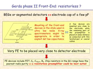
Set-up of the Gerda Experiment ΔL ≈ 10 m Electronics (Flash ADC, …) CSA ΔL ≈ 10 m Room Temperature Radioactivity issue: ∑(Material Activity * Volume) Δr2 Ge det. • CSA requirements: • Bandwidth ( > 10 MHz, 30 ns rise time) • Noise (ENC < 150 e @LNT, Tsh =10μs) • Power consumption < 50 mW/channel • Cross-talk between channels < 1% Liquid Argon Cryogenic Temperature
Set-up of the Gerda Experiment ΔL ≈ 10 m Electronics (Flash ADC, …) ??? ΔL ≈ 10 m Room Temperature CSA Radioactivity issue: ∑(Material Activity * Volume) Δr2 Ge det. • CSA requirements: • Bandwidth ( > 10 MHz, 30 ns rise time) • Noise (ENC < 150 e @LNT, Tsh =10μs) • Power consumption < 50 mW/channel • Cross-talk between channels < 1% • Cryogenic operation • Radioactivity issue: • (material, distance, volume) Liquid Argon Cryogenic Temperature
Integration = Miniaturization • CSA far from detector means: • increased noise • reduced bandwidth • increased cross-talk? From the viewpoint of the CSA design alone: closer is better 100 mm 2 mm Volume reduction ≈ 10000 Critical distance reduced by a factor of 100
Silicon Integration easy for: difficult for: • (Active Devices) • Low Noise MOS (P Type) • (< 1 nV/√Hz eq. voltage noise) • (Passive Devices) • Resistors (above 100 MOhm) • (large area or distortion with CMOS) • Capacitors (above 100 pF) • Inductors • (Active Devices) • CMOS • JFET (available technology?) • BJT (not suitable for LNT) • (Passive Devices) • Resistors (up to a few MOhm) • Capacitors (up to a few pF) also to be considered: • Interface between ASIC and outside world • (bonding wires, glue, PCB, copper shield, connectors, pins, cables, ecc.)
Components of a CSA (on paper) not easy to integrate Output Input Complete integration of a CSA with reasonable performances in terms of bandwidth, noise, power consumption, etc. is a difficult task but still possible
Components of a CSA (real world) bonding wires connector pins PCB(teflon + copper + gold) cables (teflon + copper) cables (teflon + copper) • Because cables have to be thin, they are far from ideal: • High resistivity of central wire (≈ 1 Ω/m) and shield (≈ 0.2 Ω/m) • High attenuation (10% for 10 m long cables, 50 Ω terminated) • Electro-magnetic shielding not so effective (e.g. FM radio in Milano) • Low voltage levels on board not perfectly the same as on the outside power supply
Components of a CSA (real world) decoupling capacitors • Most promising capacitors seems to be tantalum based • Number of strictly required decoupling capacitors may change across different CSAs • Reasonable values are n = 4 to 10; C = 10 μF; (VDC = 6 v) • Insufficient LVPS decoupling may generate: • noise/instability in single channel CSA • noise/instability + cross-talk in multi channels CSA
Complex Optimization Problem (example) thinner cables(less volume) integrate CSA(less volume) LVPS in parallel 3 Ch. CSA(less volume) radioactivity cross-talkdisturbancesnoise more decoupling capacitors radioactivity signal integrity 50 Ω term.receiver
Basic scenario to start with ΔL3 ΔL1 ΔL2 10 m (n) (n + 1 + 1) (n + 4 + 1) (n/2n + 4 + 1) 1 wire 2 + 1 wires 5 + 1 wires 5/6 + 1 wires CSA FE detector CSA driver receiver noise bandwidth, noise not very critical not very criticalwith receiver is 50 Ωterminated • Among open issues are: • Single or multi channels (n) CSA • Discrete or integrated electronics design • For every reasonable configuration, determine radioactivity issue ( ΔL ) • Easy to deal with mechanical design • Robustness, time, cost