Download
1 / 42
420 likes | 575 Vues
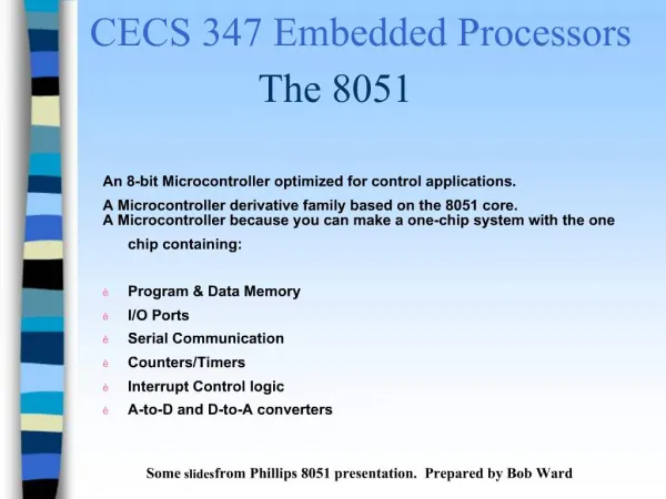
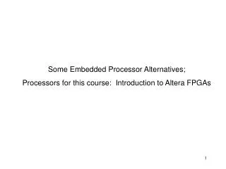
Some Embedded Processor Alternatives; Processors for this course: Introduction to Altera FPGAs. Control. I/O. Memory Data + Instruc. ALU. Processor Examples “Harvard architecture”: --PIC processor family “von Neumann architecture”: --simple processor

E N D
Some Embedded Processor Alternatives; Processors for this course: Introduction to Altera FPGAs
Control I/O Memory Data + Instruc. ALU Processor Examples “Harvard architecture”: --PIC processor family “von Neumann architecture”: --simple processor --mP 3 processor (Hamblen et al., chapter 9) --MIPS processor (Hamblen et al., chapter 14) --NIOS II processor core (Hamblen et al., chapters 15-17) Control Instruc. I/O Data ALU
PIC processor family: processor is fixed, developer programs it • Reference: http://en.wikipedia.org/wiki/PIC_microcontroller • PIC: peripheral interface controller • Originally (~1975) for offloading I/O functions from a CPU • Harvard architecture: data and instructions (“code”) are stored separately—thus a data item and an instruction do not need to be the same length • Newer versions have a stack • One accumulator (referred to as W), but memory is usually referred to as a “register file” • Some versions allow a type of indirect addressing • Usually referred to as a RISC machine; may have up to 70 instructions • May be able to access external memory (newer versions) • Many development tools & languages available Data “Code” (Instructions)
VGA port UP3 BOARD parallel port PS2 port Altera Cyclone chip USB port SRAM serial port power FLASH invalid input voltage LED on/off switch user-definable pushbuttons user-definable LEDs user-definable DIP switches +3.3V supply LED +5V supply LED global reset Some processor architectures: LC Display http://users.ece.gatech.edu/~hamblen/UP3/ and http://users.ece.gatech.edu/~hamblen/UP3/UP3%20Reference%20Manual.pdf
simple processor: • Von Neumann architecture • Only one general purpose register (accumulator) • Supports direct, indirect, and indexed addressing • Small instruction set, 2 formats (000-110 or 111) • Primitive I/O (via accumulator) • No built-in stack / stack pointer • No ability to do virtual storage M MA IR AC CF MD IA IB PC ABUS BBUS ALU ALU OUTPUT OBUS M: memory MA: memory address register MD: memory data register IR: instruction register AC: accumulator CF: carry flag IA, IB: index registers PC: program counter
mP 3 processor (Hamblen et al., chapter 9) • Similar to simple processor—von Neumann architecture, 1 accumulator • Implementation uses < 1% of Altera Cyclone device logic • Memory and I/O are now each components on the data bus; all info goes through MDR (fig. 9-1) • 8-bit instructions, 8-bit data in 1 16-bit word, several formats • Only direct addressing • Only 5 instructions given (load, store, add, jump, jneg)—can these support general-purpose computing? • No stack pointer • Can it do virtual storage?
MIPS processor (Hamblen et al., chapter 14) • Widely-used RISC architecture, 1980’s • 32-bit instructions, 3 formats • 32 general-purpose registers • 1-cycle fetch/decode/execute (employs pipelining)
NIOS II processor core (Hamblen et al., chapters 15-17) • Hardware (IP) core—SOPC example; C/C++ compiler • 32-bit datapath • 1-6 pipeline stages • 32 general purpose registers, 6 special-purpose • Optional instruction cache • Optional multiply/divide instructions • Hardware floating point unit can be added • Hardware can be customized • Development environment includes; • --C/C++ compiler • --Ability to customize library for the peripheral • devices you need
CARRY IN IN OUT BUS BUS CLOCK RESET MEM IN BUS LOGIC (LOOK-UP TABLE or LUT) MEMORY (1-BIT) MEM OUT CARRY OUT More about Altera devices and tools: Generic FPGA architecture: GLOBAL BUS FPGA (EXAMPLE) LOCAL BUS RAM BLOCK SINGLE FPGA CELL
Example: using a lookup table to describe a gate network: f(A,B,C) = A'B'C + A'BC' + A'BC + ABC (001) (010) (011) (111) Inputs: ABC out 000 0 001 1 010 1 011 1 100 0 101 0 110 0 111 1
LE (Logic Element) LAB (Logic Array Block) RAM Block
Device families: Example: “Cyclone”—we will use EP1C6 or EP1C2 features: • logic elements (LE’s) • RAM blocks • Global clock + Phase locked loops for clock configuration • >= 170 I/O pins Cyclone LE—figure 3.7 Cyclone LABs and interconnects: figure 3.9 (These references and those that follow are to the reference by Hamblen et al.)
"silicon compilation": basic idea: restrict possible physical configurations; sacrifice area / performance for "regularity" of design; use regular physical structures to enable AUTOMATION of layout All CAD tools will sacrifice some area/performance for automation and the ability to do "large" designs, just as software compilers sacrifice some efficiency for the ability to use a high-level language instead of assembly language; designer productivity will increase substantially, however SW Programming: Write Program (HLL) Link to Libraries Load/ Execute Compile Silicon Programming: Write Program (HDL/Scm) Program Device/ Execute Fit Simu-late Com-pile/ Link
Altera Project Flow (“Rapid Prototyping”): 1. (Hierarchical) DESIGN design entry schematic (mydesign.gdf) Verilog (mydesign.v) other formats (VHDL, AHDL, EDIF, ) IP cores 2.Compilation translation, optimization, synthesis (“netlist”) device fitting (placement and routing) Floorplan editor—figure 1.23 Report generation 3.”Execution” Timing analysis simulation (functional / timing) device programming, hardware verification information on power usage
VGA port UP3 BOARD parallel port PS2 port Cyclone chip USB port SRAM serial port power FLASH invalid input voltage LED on/off switch user-definable pushbuttons user-definable LEDs user-definable DIP switches +3.3V supply LED +5V supply LED global reset LC Display http://users.ece.gatech.edu/~hamblen/UP3/ and http://users.ece.gatech.edu/~hamblen/UP3/UP3%20Reference%20Manual.pdf
Technology: SRAM General description: http://en.wikipedia.org/wiki/Static_Random_Access_Memory General information on “programmable” devices: http://www.tutorial-reports.com/computer-science/fpga/user-programmability.php
Functional Testing: One more useful Altera option: note that the devices we have access to will allow us to produce fairly "large" designs. To adequately test these designs, we will need to input files of test vectors rather than relying solely on inputting waveforms (and we will need to do HIERARCHICAL design AND testing) A test vector file (myfile.vec) can be created in the text editor. Here is an example file to test a module with inputs A, B, RESET, and CLOCK and outputs X,Y,Z. A X B Y RESET Z CLOCK
INPUTS RESET ; PATTERN 0> 1 100> 0 ; OUTPUTS X Y Z ; PATTERN % check output at every Clock pulse --these are expected values% = X X X = 0 0 0 % relative time vector values % = 0 0 0 = 1 0 0 = 0 0 1 = 0 0 1 = 0 1 1 = 0 1 1 = 1 1 1 = 1 1 1 = 1 1 1 = 1 1 1 ; %test vector file for above module% % units default to ns % START 0 ; % time to start simulation% STOP 1000 ; % time to end (in ns)% INTERVAL 100 ; INPUTS CLOCK ; PATTERN 0 1 ; % pattern of clock values % % CLOCK ticks every 100 ns % INPUTS A B ; PATTERN % test every combination of % % A and B % 0> 0 0 220> 1 0 320> 1 1 % change A,B at given times % 570> 0 1 720> 1 1 ;
using the .vec file: open the simulator; then on the "File" menu choose inputs/outputs; then choose your .vec file; you must do this BEFORE opening a .scf file Note: results of the simulation cannot be saved as a .vec file. To save your results, save them as either a waveform (.vwf) or a table output (.tbl) file. Alternative: compile separately in Verilog on Sun workstations, compiler, use a testbench; then import into Altera environment; this is the standard HDl methodology (handout on this will be provided)
Useful Altera functions: • The UP3 core library • input and output for the Altera board • random number generation
UP3 functions: an IP (intellectual property) core described in chapter 5 of Hamblen et al. can be used with schematics, Verilog, or VHDL 8 modules--perform I/O “housekeeping” functions modules must be “visible” in your path or included in your design in some way (directly, package, etc.)
output input
VGA port UP3 BOARD parallel port PS2 port Cyclone chip USB port SRAM serial port power FLASH invalid input voltage LED on/off switch user-definable pushbuttons user-definable LEDs user-definable DIP switches +3.3V supply LED +5V supply LED global reset LC Display http://users.ece.gatech.edu/~hamblen/UP3/ and http://users.ece.gatech.edu/~hamblen/UP3/UP3%20Reference%20Manual.pdf
COMPONENT LCD_Display PORT (Hex_Display_Data: IN STD_LOGIC_VECTOR (Num_Hex_Digists*4)-1 DOWNTO 0; reset, clock_48MHz: IN std_logic; LCD_RS, LCD_E: OUT STD_LOGIC; DATA_BUS: INOUT STD_LOGIC_VECTOR (7 DOWNTO 0); END COMPONENT; input 4 bits hex digit signal values to convert to ASCII hex digits and send to LED display (note: Appendix D contains ASCII to hex table) Num_Hex_Digits is a Generic parameter which can be given a value in a VHDL file or in a schematic (16 characters, 2 lines available) Outputs PIN (important!) LCD_RS 108 LCD_E 50 LCD_RW 73 DATA_BUS (7 DOWNTO 0): 113, 106, 104, 102, 100, 98, 96, 94
COMPONENT Debounce PORT (pb, clk_100Hz:IN STD_LOGIC; pb_debounced:OUT STD_LOGIC); END COMPONENT; pb is the input from a pushbutton (see I/O pins, chapter 2) since pushbuttons have a mechanical “bounce”, this component samples the input over several clock cycles and filters out the bounces; it will register the pushbutton input only when several sequential samples of the input agree the clock input is used by the bounce filter (see example below) when “push” is registered, output goes low: it remains low until button is released
COMPONENT OnePulse PORT (PB_debounced, clock:IN STD_LOGIC; PB_single_pulse:OUT STD_LOGIC); END COMPONENT; after the push button signal is “debounced”, this component can be used to ensure that the output read from the pushbutton is high for only one clock cycle, no matter how long the pushbutton is held down this is useful for building finite state machines--an edge-triggered flip-flop can be used to build a state and each input will be active for only one clock cycle the “clock” input is the clock signal being used to drive the state machine
COMPONENT Clk_Div PORT ( clock_48MHz: IN STD_LOGIC; clock_1MHz, clock_100KHz, clock_10KHz, clock_1KHz, clock_100Hz, clock_10Hz, clock_1Hz: OUT STD_LOGIC) END COMPONENT; the input is from the (48MHz) on-board clock (pin 29 for the Cyclone chip); JP3 jumper must be set to select the 48MHz USB—this the default setting the outputs are clock signals of various frequencies which can be used in designs Note: actual frequency will be (listed frequency)*(1.007 +/- .005%)
Example: pushbutton fsm Debounce OnePulse Clock (pin 29) Clock_100Hz Clk_Div Clock_1MHz
COMPONENT Mouse PORT ( clock_48Mhz,reset: IN STD_LOGIC; mouse_data, mouse_clk:INOUT STD_LOGIC; left_button,right_button: OUT STD_LOGIC; mouse_cursor_row,mouse_cursor_column: OUT STD_LOGIC_VECTOR(9 DOWNTO 0); END COMPONENT; the input is from the (48MHz) on-board clock (pin 29 for the Cyclone chip); mouse_data is pin 13, mouse_clk is pin 12: BIDIRECTIONAL (also used for keyboard) cursor outputs give postion in 640 x 480 pixel screen (VGA); cursor is initialized to the middle of the screen button outputs are high when the corresponding button is pushed
COMPONENT Keyboard PORT ( keyboard_clk,keyboard_data, clock_48Mhz, reset, read: IN STD_LOGIC; scan_code: OUT STD_LOGIC_VECTOR(7 DOWNTO 0); scan_ready: OUT STD_LOGIC); END COMPONENT; Reads PS/2 keyboard scan code; converts serial data from keyboard to parallel clock input is from the (48MHz) on-board clock (pin 29 for the Cyclone chip); keyboard_data is pin 13, keyboard_clk is pin 12: INPUTS (also used for mouse) read clears the scan_ready signal; reset clears flip-flops for serial-to-parallel conversion scan_code: table of values in Table 11.3; --”make” code: key is hit; “break” code: key is released ex: ‘A’ make = 1C, break = F01C: ‘shift’ make = 12, break = F012 (if key is held down, several makes will be sent before a break) scan_ready goes high when new scan code is sent and can be used to make sure each scan code is read only once
COMPONENT VGA_Sync PORT (clock_48MHz, red, green, blue: IN STD_LOGIC; red_out, green_out, blue_out, horiz_sync_out, vert_sync_out: OUT STD_LOGIC; pixel_row, pixel_column: OUT STD_LOGIC_VECTOR(9 DOWNTO 0)); END COMPONENT; clock_48MHz signal must come from pin 29 (Cyclone chip) user logic generates the input “color” (red, green, blue) Cyclone chip: horiz_sync --> pin 226, vert_sync --> pin 227 red_out --> pin 228, green_out --> pin 122, blue_out --> pin 170 pixel_row and pixel_column give the pixel address how many colors are available? how many pixels? (“dithering”: one color on odd cycles, different on even twice as many colors example: pattern sent (even/odd cycles) pattern observed
COMPONENT Char_ROM PORT (clock: IN STD-logic; character_address: IN STD_LOGIC_VECTOR (5 DOWNTO 0); font_row, font_col: IN STD_LOGIC_VECTOR (2 DOWNTO 0); row_mux_output: OUT STD_LOGIC); END COMPONENT; generates text for a video display--each character requires an 8 x 8 pixel pattern (see codes, table 9.1--a memory initialization file, tcgrom.mif, is provided; the font data can be stored in one M4K memory block) character_address addresses the character to be displayed font_row and font_col step through the 64 pixels (8x8) needed to display one character Clock loads the address register and should be tied to the video pixel_clock row_mux_output is the pixel value to be output for this character at this position and can be used to generate the correct RGB pixel color
640 480 How does output occur (examples: chapter 10): monitor contains CRT (cathode ray tube) screen consists of pixels, 640 in a row and 480 in a column (VGA format) “refresh rate”: how quickly these pixels are scanned standard rate is 60 times / second (60 Hz) (human eye can detect “flicker” below 30Hz) if there are 640 X 480 pixels, with a 60Hz refresh rate, how much time is available to scan one pixel? What clock speed is therefore required? What is the onboard clock speed? (note: UP3 has PLL which can be used to obtain faster refresh rates) Sync signals tell when to start a new row or column
random number generation (Appendix A): actually generates “pseudorandom” numbers Q: what is the difference? Method: example: n = 32--will give 32-bit pseudorandom sequence of bits from table, read “XOR from bits 32,22,2,1” (bits are 32--1, not 31--0) build a 32-bit shift register that shifts left one bit per cycle next bit to be input into lsb should be the XOR of bits 32,22,2,1 this will generate a sequence in “pseudorandom order” initial value in the register is the “seed”; 0 should not be used (why?)
Example: n = 3--table gives bits 3,2 step pattern (bit 3) xor (bit 2) 0 111 0 1 110 0 2 100 1 3 001 0 4 010 1 5 101 1 6 011 1 7 111 0---from here, the sequence will repeat we have a sequence of the numbers 1-7: 7,6,4,1,2,5,3 this is the longest nonrepeating sequence we can have order will always be the same, seed only determines where we start
How good are the random numbers generated? Reference: Shruthi Narayanan, M.S. 2005, ATI Technologies Hardware implementation of genetic algorithm modules for intelligent systems: Random numbers generated by one shift register Random numbers generated by multiple shift registers