Download
1 / 12
120 likes | 319 Vues
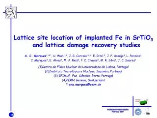
Lattice site location of implanted Fe in SrTiO 3 and lattice damage recovery studies. A. C. Marques 1,4 * , U. Wahl 1,2 , J. G. Correia 1,2,4 , E. Rita 1,2 , J. P. Araújo 3 , L. Pereira 3 , C. Marques 2 , E. Alves 2 , M. A. Reis 2 , P. C. Chaves 2 , M. R. Silva 1 , J. C. Soares 1

E N D
Lattice site location of implanted Fe in SrTiO3 and lattice damage recovery studies A. C. Marques1,4 *, U. Wahl1,2, J. G. Correia1,2,4, E. Rita1,2, J. P. Araújo3, L. Pereira3, C. Marques2, E. Alves2, M. A. Reis2, P. C. Chaves2, M. R. Silva1, J. C. Soares1 (1)Centro de Física Nuclear da Universidade de Lisboa, Portugal(2)Instituto Tecnológico e Nuclear, Sacavém, Portugal(3) IFIMUP, Fac. Ciências, Porto, Portugal (4)CERN, Geneva, Switzerland * ana.marques@cern.ch
Outline • Materials, • Undoped SrTiO3 • SrTiO3 pre-implanted with stable Fe emission channeling technique, studies • Fe lattice site location • lattice damage recovery • Magnetic properties • impurities search by means of PIXE • and conclusions.
Why studying SrTiO3? • Because … • High bulk dielectric constant microelectronic applications (ex. high-k FET). • interesting and complex electrical, optical and magnetic properties that can be modified by the incorporation of dopants (ex. Fe-doped SrTiO3 has been applied in electrochemical electrodes and resistive oxygen sensors ) • Transition metal doped SrTiO3 is a possible material for a RT ferromagnetic semiconductor Spintronics applications • Variety of phase transitions in the low temperature range • Besides, • little is known on the lattice site location of implanted impurities and remaining point defects in heir neighborhood. EC and PAC can give unique answers in that respect!
Electron Emission Channeling 2D emission patterns characterizes specific lattice sites of the emitting atoms (accuracy up to 0.1 Ǻ) (a) (a) When electrons are emitted from substitutional impurities, there will be achanneling effect: electrons ere preferentially steered along this row of atoms, resulting in a higher anisotropy. (b) (b) When electrons are emitted from interstitial impurities there will bechanneling and blocking effects that will decrease the anisotropy when looking along the row of atoms.
On-line set-up for short-lived isotopes Experimental set-up Off-line set-up Table: Some radioactive isotopes for possible future use with the EC technique:
Linux USB . . . Chip (Front-End) VME Card Interface Module Si Pad detector IB e- PCB 111In 181Hf VATA-DAQ as a readout system INTEGRAL SPECTRA - NOT GAIN CALIBRATED lowest detectable energy 13.4 keV FWHM @ 17.4 keV 1.18 keV 145 keV 219 keV 65 keV - K 122 keV - L 131keV - M 168 keV 242 keV • Lowest 111In electron energy of 145 keV has an FWHM of 4.8 keV! • Lowest energy that can be detected with this PSD is 15 KeV!
mixed <111> Ti row octahedral interstitial site Sr row <001> <110> <001> <110> EC results – 59Fe:SrTiO3 Undoped sample ion implantation details Where: ISOLDE, CERN (Geneva) Energy: 60 keV Dose: 2×10¹³ at./cm2 EC measurements: patterns were recorded along 4 directions in the as-implanted state and after annealing at 300ºC, 600ºC, 750ºC and 900ºC. Results Angular distributions “@” 900ºC
Crystalline quality for <100>: Virgin samp. 1.9% STO+1x10¹⁵ Fe at.cm2 8.5% STO+5x10¹⁵ Fe at.cm2 9% random <111> <110> <100> <100> <111> <110> SrTiO3 lattice characterization by RBS/Channeling Crystalline directions under study: After 900ºC annealing
Magnetic measurements performed with a SQUID MPMS EverCool System Automated control of temperature, magnetic field and helium liquefaction
Magnetic measurements performed with a SQUID 10 K 5.5 T 5.26x10¹⁵ Fe at./cm2 Magnetic measurements were performed in two SrTiO3 samples pre-implanted with stable Fe at ITN-Portugal and after 900ºC vacuum annealing. Low dose sample 1.69x10¹⁵ at./cm2 High dose sample 5.26 x10¹⁵ at./cm2 Undoped sampleas sensitized 1.69x10¹⁵ Fe at./cm2 Fe 2.2 B Fe2+ 6 B Fe3+ 5 B M = 8,8 B/Fe M is considerably higher!! Why?? … we still don’t know! is normalized to the mass sample
Cu paramagnetic impurity (Cu2+)/ion = 1.7 B Impurities search in SrTiO3 by means of PIXE PIXE analysis revealed the following: • Absence of Cu impurities in the Virgin sample Zoom
Summary / Future work • Emission Channeling • up to 900ºC 59Fe atoms preferentially go to Ti-near sites (86%). • RBS/Channeling Spectroscopy • Good crystalline quality samples • after Fe-doping and 900ºC post-annealing there are still remaining defects in the sample. • SQUID Measurements • The magnetic properties are modified by the introduction of Fe dopant to different doses. • Magnetization increases with Fe concentration but to a value bigger than what would be expected. • Why? We still don’t know but the following questions comes up: • What is the Fe atoms valence in the crystal? • Are the remaining defects playing a role? Or clusters have been formed after the annealing? • FUTURE WORK: Future work at ISOLDE will be to study 65Ni (2.5 h) and 61Co (1.5 h) lattice site location in SrTiO3 and other oxides.