Memory part 2: Organization
Memory part 2: Organization. Dr. Doug L. Hoffman Computer Science 330 Spring 2000. From Last Time: the Memory Hierarchy. Present the user with as much memory as is available using the cheapest technology. Provide access at the speed offered by the fastest technology.

Memory part 2: Organization
E N D
Presentation Transcript
Memory part 2: Organization Dr. Doug L. Hoffman Computer Science 330 Spring 2000
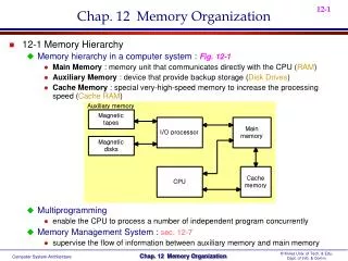
From Last Time: the Memory Hierarchy • Present the user with as much memory as is available using the cheapest technology. • Provide access at the speed offered by • the fastest technology. Processor Control Tertiary Storage (Disk) Secondary Storage (Disk) Second Level Cache (SRAM) Main Memory (DRAM) On-Chip Cache Datapath Registers
Main Memory Background • Performance of Main Memory: • Latency: Cache Miss Penalty • Access Time: time between request and word arrives • Cycle Time: time between requests • Bandwidth: I/O & Large Block Miss Penalty (L2) • Main Memory is DRAM: Dynamic Random Access Memory • Dynamic since needs to be refreshed periodically (8 ms) • Addresses divided into 2 halves (Memory as a 2D matrix): • RAS or Row Access Strobe • CAS or Column Access Strobe • Cache uses SRAM: Static Random Access Memory • No refresh (6 transistors/bit vs. 1 transistorSize: DRAM/SRAM 4-8, Cost/Cycle time: SRAM/DRAM 8-16
Random Access Memory (RAM) Technology • Why do computer designers need to know about RAM technology? • Processor performance is usually limited by memory bandwidth • As IC densities increase, lots of memory will fit on processor chip • Tailor on-chip memory to specific needs • Instruction cache • Data cache • Write buffer • What makes RAM different from a bunch of flip-flops? • Density: RAM is much more denser
Static RAM Cell 6-Transistor SRAM Cell word word (row select) 0 1 • Write: 1. Drive bit lines (bit=1, bit=0) 2.. Select row • Read: 1. Precharge bit and bit to Vdd 2.. Select row 3. Cell pulls one line low 4. Sense amp on column detects difference between bit and bit 0 1 bit bit bit bit
Wr Driver & Precharger Wr Driver & Precharger Wr Driver & Precharger Wr Driver & Precharger - + - + - + - + - + - + - + - + Sense Amp Sense Amp Sense Amp Sense Amp Typical SRAM Organization: 16-word x 4-bit Din 3 Din 2 Din 1 Din 0 WrEn Precharge A0 Word 0 SRAM Cell SRAM Cell SRAM Cell SRAM Cell A1 Address Decoder A2 Word 1 SRAM Cell SRAM Cell SRAM Cell SRAM Cell A3 : : : : Word 15 SRAM Cell SRAM Cell SRAM Cell SRAM Cell Dout 3 Dout 2 Dout 1 Dout 0
The Problem with SRAM Select = 1 • Six transistors use up a lot of area P1 P2 Off On On On On Off N1 N2 bit = 1 bit = 0
1-Transistor Memory Cell (DRAM) row select • Write: • 1. Drive bit line • 2.. Select row • Read: • 1. Precharge bit line • 2.. Select row • 3. Cell and bit line share charges • Very small voltage changes on the bit line • 4. Sense (fancy sense amp) • Can detect changes of ~1 million electrons • 5. Write: restore the value • Refresh • 1. Just do a dummy read to every cell. bit
Classical DRAM Organization (square) bit (data) lines r o w d e c o d e r Each intersection represents a 1-T DRAM Cell • Row and Column Address together: • Select 1 bit a time RAM Cell Array word (row) select Column Selector & I/O Circuits row address Column Address data
DRAM Performance • A 60 ns (tRAC) DRAM can • perform a row access only every 110 ns (tRC) • perform column access (tCAC) in 15 ns, but time between column accesses is at least 35 ns (tPC). • In practice, external address delays and turning around buses make it 40 to 50 ns • These times do not include the time to drive the addresses off the microprocessor nor the memory controller overhead. • Drive parallel DRAMs, external memory controller, bus to turn around, SIMM module, pins… • 180 ns to 250 ns latency from processor to memory is good for a “60 ns” (tRAC) DRAM
Main Memory Performance • Simple: • CPU, Cache, Bus, Memory same width (32 bits) • Wide: • CPU/Mux 1 word; Mux/Cache, Bus, Memory N words (Alpha: 64 bits & 256 bits) • Interleaved: • CPU, Cache, Bus 1 word: Memory N Modules(4 Modules); example is word interleaved
Cycle Time versus Access Time Cycle Time Access Time Time • DRAM (Read/Write) Cycle Time >> DRAM (Read/Write) Access Time • 2:1 • DRAM (Read/Write) Cycle Time : • How frequent can you initiate an access? • Analogy: A little kid can only ask parent for money on Saturday • DRAM (Read/Write) Access Time: • How quickly will you get what you want once you initiate an access? • Analogy: As soon as asked, the parent will give him the money • DRAM Bandwidth Limitation analogy: • What happens if he runs out of money on Wednesday?
Increasing Bandwidth - Interleaving Access Pattern without Interleaving: CPU Memory D1 available Start Access for D1 Start Access for D2 Memory Bank 0 Access Pattern with 4-way Interleaving: Memory Bank 1 CPU Memory Bank 2 Memory Bank 3 Access Bank 1 Access Bank 0 Access Bank 2 Access Bank 3 We can Access Bank 0 again
Main Memory Performance • Timing model • 1 to send address, • 6 access time, 1 to send data • Cache Block is 4 words • Simple M.P. = 4 x (1+6+1) = 32 • Wide M.P. = 1 + 6 + 1 = 8 • Interleaved M.P. = 1 + 6 + 4x1 = 11
Independent Memory Banks • How many banks? number banks number clocks to access word in bank • For sequential accesses, otherwise will return to original bank before it has next word ready • Increasing DRAM => fewer chips => harder to have banks • Growth bits/chip DRAM : 50%-60%/yr • Nathan Myrvold M/S: mature software growth (33%/yr for NT) growth MB/$ of DRAM (25%-30%/yr)
32 8 8 2 4 1 8 2 4 1 8 2 Fewer DRAMs/System over Time DRAM Generation ‘86 ‘89 ‘92 ‘96 ‘99 ‘02 1 Mb 4 Mb 16 Mb 64 Mb 256 Mb 1 Gb 4 MB 8 MB 16 MB 32 MB 64 MB 128 MB 256 MB Memory per DRAM growth @ 60% / year 16 4 Minimum PC Memory Size Memory per System growth @ 25%-30% / year
N cols RAS_L Page Mode DRAM: Motivation Column Address • Regular DRAM Organization: • N rows x N column x M-bit • Read & Write M-bit at a time • Each M-bit access requiresa RAS / CAS cycle • Fast Page Mode DRAM • N x M “register” to save a row DRAM Row Address N rows M bits M-bit Output 1st M-bit Access 2nd M-bit Access CAS_L A Row Address Col Address Junk Row Address Col Address Junk
N cols Fast Page Mode Operation Column Address DRAM • Fast Page Mode DRAM • N x M “SRAM” to save a row • After a row is read into the register • Only CAS is needed to access other M-bit blocks on that row • RAS_L remains asserted while CAS_L is toggled Row Address N rows N x M “SRAM” M bits M-bit Output 1st M-bit Access 2nd M-bit 3rd M-bit 4th M-bit RAS_L CAS_L A Row Address Col Address Col Address Col Address Col Address
DRAM Design Goals • Reduce cell size 2.5, increase die size 1.5 • Sell 10% of a single DRAM generation • 6.25 billion DRAMs sold in 1996 • 3 phases: engineering samples, first customer ship(FCS), mass production • Fastest to FCS, mass production wins share • Die size, testing time, yield => profit • Yield >> 60% (redundant rows/columns to repair flaws)
DRAM History • DRAMs: capacity +60%/yr, cost –30%/yr • 2.5X cells/area, 1.5X die size in 3 years • ‘97 DRAM fab line costs $1B to $2B • DRAM only: density, leakage v. speed • Rely on increasing no. of computers & memory per computer (60% market) • SIMM or DIMM is replaceable unit => computers use any generation DRAM • Commodity, second source industry => high volume, low profit, conservative • Little organization innovation in 20 years page mode, EDO, Synch DRAM • Order of importance: 1) Cost/bit 1a) Capacity • RAMBUS: 10X BW, +30% cost => little impact
Today’s Situation: DRAM • Commodity, second source industry high volume, low profit, conservative • Little organization innovation (vs. processors) in 20 years: page mode, EDO, Synch DRAM • DRAM industry at a crossroads: • Fewer DRAMs per computer over time • Growth bits/chip DRAM : 50%-60%/yr • Nathan Myrvold M/S: mature software growth (33%/yr for NT) growth MB/$ of DRAM (25%-30%/yr) • Starting to question buying larger DRAMs?
Today’s Situation: DRAM $16B $7B • Intel: 30%/year since 1987; 1/3 income profit
Summary: Processor-Memory Performance Gap “Tax” Processor % Area %Transistors (cost) (power) • Alpha 21164 37% 77% • StrongArm SA110 61% 94% • Pentium Pro 64% 88% • Caches have no inherent value, only try to close performance gap
Summary: • Two Different Types of Locality: • Temporal Locality (Locality in Time): If an item is referenced, it will tend to be referenced again soon. • Spatial Locality (Locality in Space): If an item is referenced, items whose addresses are close by tend to be referenced soon. • By taking advantage of the principle of locality: • Present the user with as much memory as is available in the cheapest technology. • Provide access at the speed offered by the fastest technology. • DRAM is slow but cheap and dense: • Good choice for presenting the user with a BIG memory system • SRAM is fast but expensive and not very dense: • Good choice for providing the user FAST access time.