SERIAL PERIPHERAL INTERFACE (SPI)
SERIAL PERIPHERAL INTERFACE (SPI). Module Objective. Understand SPI format and data transfersgure the control registers Transmit and receive data Module exercise: Configure the SPI to transmit and receive characters to/from another device in Master mode at a 1 MHz rate. IRQ. LVI. Direct

SERIAL PERIPHERAL INTERFACE (SPI)
E N D
Presentation Transcript
Module Objective • Understand SPI format and data transfersgure the control registers • Transmit and receive data • Module exercise: Configure the SPI to transmit and receive characters to/from another device in Master mode at a 1 MHz rate
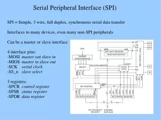
IRQ LVI Direct Memory Access Module (DMA) System Integration Module (SIM) Clock Generation Module (CGM) Timer Interface Module (TIM) 68HC08 CPU RESET COP BREAK Internal Bus (IBUS) Random Access Memory (RAM) Serial Peripheral Interface (SPI) Electronically Programmable ROM Monitor ROM Serial Communications Interface (SCI) SERIAL PERIPHERAL INTERFACE MODULE • Features of the SPI module include the following: • Full-Duplex Operation • Master and Slave Modes • Separate Transmit and Receive Registers • Four Master Mode Frequencies (Maximum = Bus Frequency 2) • Maximum Slave Mode Frequency = Bus Frequency • Separate Clock Ground for Reduced Radio Frequency (RF) Interference • Serial Clock with Programmable Polarity and Phase • Bus Contention Error Flag • Overrun Error Flag • Two Separately Enabled Interrupts with DMA or CPU Service: • SPRF (SPI Receiver Full) • SPTE (SPI Transmitter Empty) • Programmable Wired-OR Mode • I2C (Inter-Integrated Circuit) Compatibility
SPI I/O Registers • Three registers control and monitor SPI operations: • SPI Control Register (SPCR) • SPI Status and Control Register (SPSCR) • SPI Data Register (SPDR)
SPI Modes • Master mode • Only a master SPI initiates a transmission • Data is shifted out via Master Out Slave In (MOSI) line • Data is shifted in via Master In Slave Out (MISO) line • Transmission ends after 8 cycles of serial clock (SPSCK) • Slave Mode • Transfer synchronized to serial clock (SPSCK) from Master • Data is shifted in via the Master Out Slave In (MOSI) line • Data is shifted out via the Master In Slave Out (MISO) line
MASTER SLAVE MOSI MISO Shift Register Shift Register SPSCK +5v SS Baud Rate Gen. SS Slave Select Pin • Slave Select (SS) • Master mode • SS held high during transmission • Acts as error detection input • Can be general purpose output • Slave mode • SS must remain low until transmission completes 0 = Enables slave 1 = Disables slave
READ: SPCR SPRIE DMAS SPMSTR CPOL CPHA SPWOM SPE SPTIE WRITE: RESET: 0 0 0 0 1 0 0 0 SPI Control Register • SPI Control Register (SPCR) • SPI Master (SPMSTR) • Selects master mode or slave mode operation 1 = Master mode 0 = Slave mode • SPI Master and Slave need identical clock polarity and phase settings • Clock Polarity (CPOL) • Determines clock state when idle • Clock Phase (CPHA) 1 = Begin capturing data on second clock cycle edge 0 = Begin capturing data on first clock cycle edge* • When CPHA = 0, the SS must be deasserted and reasserted between each transmitted byte • SPI Enable (SPE) • 1 = SPI module enabled • 0 = SPI module disabled • Recommend disabling SPI before initializing or changing clock phase, clock polarity, or baud rate
SS CPHA CPOL 0 0 SPSCK 1 0 SPSCK 1 0 SPSCK 1 1 SPSCK MSB Bit 6 Bit 4 Bit 3 Bit 2 LSB MOSI/MISO Bit 5 Bit 1 Capture Strobe Clock Polarity and Phase • SPI Control Register (SPCR) • SPI modules need identical Clock polarity and phase
Baud Rate System Clock SPR1:SPR0 Divided By (System Clock Freq. = 8 MHz) 2 00 4 MHz 1 MHz 8 01 32 250 KHz 10 11 128 62.5 KHz SPI Baud Rate 0 READ: SPRF 0 OVRF MODF SPTE SPR1 SPR0 SPSCR WRITE: • SPI Status and Control Register (SPSCR) • SPI rate select bits (SPR1, SPR0) • Sets the Master SPSCK clock frequency • No effect in the Slave devices • Baud Rate = CGMOUT / Baud Rate Divisor RESET: 0 0 0 0 1 0 0 0
READ: Bit 7 Bit 6 Bit 5 Bit 4 Bit 3 Bit 2 Bit 1 Bit 0 SPDR WRITE: RESET: UNAFFECTED BY RESET SPI Data Register • SPI Data Register (SPDR) • Read/Write buffer for SPI data • Write operation • Writes data to transmit data register • Read operation • Reads data in receive data register
SPI Status Flags 0 READ: SPRF 0 OVRF MODF SPTE SPSCR SPR1 SPR0 • SPI Status and Control Register (SPSCR) • SPI Receiver Receiver Full (SPRF) • Set when a byte is shifted from shift register to the receive data register • Cleared by reading SPSCR then reading SPDR 1 = Receive data register full 0 = Receive data register not full • SPI Transmitter Empty (SPTE) • Set when a byte is transferred from SPDR to the shift register • Cleared by reading SPDR register 1 = Transmit data register empty 0 = Transmit data register not empty WRITE: RESET: 0 0 0 0 1 0 0 0
SPI Interrupts READ: SPCR SPRIE DMAS SPMSTR CPOL CPHA SPWOM SPE SPTIE WRITE: • SPI Control Register (SPCR) • SPI Receiver Interrupt Enable Bit (SPRIE) • Interrupt generated when SPRF flag set • SPI Transmit Interrupt Enable (SPTIE)) • Interrupt generated when SPTE flag set 1 = Interrupt enabled 0 = Interrupt disabled • Direct Memory Access Select (DMAS) • Selects either DMA or CPU interrupt request • SPRIE/SPTIE bits still enable or disable interrupts RESET: 0 0 0 0 1 0 0 0
Initialization • SPI Initialization sequence • 1) Initialize SPI clock frequency ( SPR1 and SPR0 in SPSCR ) • 2) Set clock configuration ( CPOL and CPHA bits in SPSCR ) • 3) Select Master/Slave operation ( SPMSTR in SPCR ) • 4) Enable interrupts if desired ( SPTIE, SPRIE in SPCR ) • 5) Enable the SPI system ( SPE in SPCR ) • Should enable Master before Slaves
Master to Slave Transfer • Simple Polled operation • 1) Initialize the SPI • 2) Select SS to Slave device (hardware dependent • 3) Write byte to SPDR • 4) Wait for SPI Transmitter Empty Flag (SPTE) • 5) Read the SPDR • 6) Release SS to Slave (hardware dependent)
SPI Exercise • Part 1: Initialize a SPI to the following: Master mode 1 MHz baud rate ( 8 MHz system clock ) Clock phase = 1 and clock polarity = 0 Polled operation • Part 2: Write a procedure to transmit the character in the Accumulator to the Slave device. Then wait for the received character and place it into the Accumulator. (The Master SS is tied to VDD and the Slave SS is tied to ground)
Additional InformationWired-Or Mode READ: • SPI Control Register (SPCR) • SPI Wired OR Mode (SPWOM) • Configures MISO, MOSI, and SPSCK outputs to be open-drain drivers • Allows multiple-master systems • Provides some protection against CMOS latchup SPCR SPRIE DMAS SPMSTR CPOL CPHA SPWOM SPE SPTIE WRITE: RESET: 0 0 0 0 1 0 0 0
Additional InformationOverflow and Mode Fault Status Flags 0 READ: SPRF 0 OVRF MODF SPTE • SPI Status and Control Register (SPSCR) • Overflow flag (OVRF) • Failure to read data register before it is over written • Incoming data bytes are lost • Data register contents unaffected • Cleared by reading the data register • Mode Fault flag (MODF) • Master mode only • Indicates another master tried to access this device • Set when another device pulls SS pin low • Cleared by a write to the SPSCR SPSCR SPR1 SPR0 WRITE: RESET: 0 0 0 0 1 0 0 0
Additional InformationLow Power Modes • Low Power Modes • WAIT • SPI mode remains active • SPI registers are not accessible • Except by DMA • Enabled SPI interrupts will exit wait mode • STOP • SPI module becomes inactive • No affect on register conditions • Operation continues after an external interrupt
SPRIE READ: DMAS SPCR SPMSTR CPHA SPWOM CPOL SPE SPTIE WRITE: READ: Bit 7 Bit 6 Bit 5 Bit 4 Bit 3 Bit 2 Bit 1 Bit 0 SPDR WRITE: Register Summary READ: MODF SPTE SPRF 0 OVRF 0 SPSCR SPR1 SPR0 WRITE: