Download
1 / 4
40 likes | 153 Vues
Structure of a Pentacene Monolayer Deposited on SiO 2 : Role of Trapped Interfacial Water. Randall L. Headrick, University of Vermont, DMR0348354. Significance

E N D
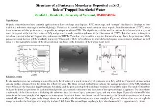
Structure of a Pentacene Monolayer Deposited on SiO2: Role of Trapped Interfacial Water Randall L. Headrick, University of Vermont, DMR0348354 Significance Organic semiconductors have potential applications in low-cost large area displays, RFID smart tags, and “e-paper” displays (i.e. displays on non-traditional substrates that require no backlighting). Pentacene is a model organic semiconductor since organic thin film transistors (OTFTs) made from pentacene exhibit performance comparable to amorphous silicon TFTs. The significance of this work is that we have learned that a layer of water is trapped at the interface between SiO2 and pentacene under condition relevant to the fabrication of OTFTs. Interface water is thought to introduce trap states that will degrade the performance of OTFTs. Therefore, if we can find a way to eliminate the water layer, the performance if the pentacene-based devices will be markedly improved. This result is likely to be relevant to other dielectric/organic semiconductor interfaces as well, since it is the hydrophilic nature of the silicon dioxide that leads to the formation of the trapped water layer. Research results In situ synchrotron x-ray scattering was used to probe the structure of a single monolayer of pentacene on a SiO2 substrate. Figure (a) shows electron density profiles obtained from the fitting the reflectivity data. The three vertical dashed lines indicate the average positions of the SiO2/interfacial water boundary, the hydration layer/pentacene boundary, and the pentacene/top hydration layer boundary, from left to right. The small vertical bars indicate the interface positions for each individual profile. A systematic variation of the thickness of the top water layer is apparent. The inset shows a schematic of the film structure, including the substrate, interface water layer, pentacene layer, and top water layer. Figure (b) showsAFM data taken from the same sample after exposure to atmosphere for several hours. An almost closed first monolayer is formed in coexistence with some second ML nuclei. The region in the image shows an area where the island coalescence is not complete. Figure (c) shows a line scan through the image shows that the first layer step height h1 is about 2.4-2.5 nm. The second layer step height h2 is also shown,which is approximately 1.6 nm.
Roughness Asymmetry in WSi2/Si Multilayers Randall L. Headrick, University of Vermont, DMR0216704 DMR0348354 Aim of the project Amorphous multilayers have many applications in x-ray optical devices for x-ray microscopy, x-ray astronomy, x-ray lithography, and x-ray microanalysis. WSi2/Si multilayers are a promising candidate system for the production of x-ray Laue focusing lenses with nanometer-scale line or point focus (Figure (a)). The main objective of this research is to investigate the interface and surface morphology of the WSi2/Si multilayers and to understand the fundamental mechanisms of roughening and smoothing that occur during the WSi2/Si multilayers deposition. Research results Amorphous WSi2 and Si were prepared by dc magnetron sputtering in an ultra high vacuum chamber. A series of x-ray scattering measurements were performed during the deposition including real-time specular/off-specular intensity monitoring, and in-situ reflectivity scans after each deposited layer. Real-time scattering intensity oscillation during Si film deposition indicate that the surface rapidly roughens as the Si grows thicker. However, when WSi2 was subsequently deposited on this rough Si layer, we found that the high-frequency surface roughness initially present on the Si surface is gradually smoothed out on the WSi2 growth surface. This is due to the strong smoothing mechanism taking place in the WSi2 growth process, which leads to an alternately smooth and rough interface structure in WSi2/Si multilayers, which is depicted in Figure (b). Energetic particles assisting the growth may play a role in inducing this asymmetry in the interface roughness. The results are notable because by understanding the fundamental mechanisms of roughening and smoothing during the deposition, WSi2/Si multilayers for multilayer Laue lens applications can be produced with reduced interfacial roughness and high performance. Multilayer Laue lens x-ray Si wafer (a) (b) LegendFigure (a)-Schematic cross section through a depth-graded multilayer laue lens. A transmission diffraction geometry is used- the x-ray beam enters from the left and is focused to the right. (Chian Liu et al. J. Appl. Phys. 98, 113519,2005) Figure (b)-Schematic sketch of an alternately smooth and rough interface structure in WSi2/Si multilayers.
Reciprocal Space Map (b) Wavelength Tunability of Self-organized Nanostructures on Surfaces Randall L. Headrick, University of Vermont, DMR0216704 DMR0348354 Aim of the project In this project, a study of ion-bombardment induced ripples on sapphire surfaces was carried out to investigate the mechanism underlying the mask-free pattern formation. Patterns formed through this bombardment induced self-organization process provides great potentials for exploring novel nanoscale phenomenon. Research Results Surface characterization by in-situ synchrotron x-ray diffuse scattering and ex-situ atomic force microscopy are performed to study the wavelength of sapphire ripples. This phenomenon has been determined to arise from a competition between irradiation-induced roughening and several smoothing mechanisms. Strong smoothing near normal incidence is inferred from the observation that the ripple wavelength becomes larger as the incidence angle is reduced. As a result of this study, we have learned how to control the wavelength of one-dimensional ripple structures formed on sapphire from 2000 nm down to 20 nm. The results are notable because the wide range of tunability allows wavelength-specific studies of the fundamental mechanism of surface evolution during film growth and surface processing with ion beams and plasmas. It also provides an easy route to tune the size of self-organized nanostructures for spintronic and opto-electronic applications. AFM Ar+ beam direction (a) Legend (a) 500 nm atomic force microscope image of the surface showing a ripple structure with a 30 nm wavelength. (b) Off-specular x-ray diffuse scattering reciprocal space map of a rippled surface. X-ray data were collected with a custom-built instrument at the National Synchrotron Light Source at Brookhaven National Laboratory, beamline X21.
Working Model of a Scanning Probe Microscope for an Introductory Nanoscience Lab Randall L. Headrick, University of Vermont, DMR0348354 In order to explain the working principles of an atomic force microscope (AFM) to an introductory level nanoscience class, we have created an inexpensive model for an AFM scanning probe microscope using a modified phonograph stylus in place of the AFM cantilever and tip. The upper photograph shows first year students working with the microscope during the teaching lab. The microscope was designed by an undergraduate physics major, Kirsten Bonson. The design and results of the project were presented at the Fall 2005 joint meeting of the New-England Sections of the American Physical Society and American Association of Physics Teachers, held in Burlington, VT (lower picture).