Quantum Tunneling Field Effect Transistors Without Semiconductors
A breakthrough method demonstrates TFETs without semiconductors using insulating boron nitride nanotubes functionalized with gold quantum dots. This new approach offers reduced power consumption and leakage current. Microscopic images and research details are provided.

Quantum Tunneling Field Effect Transistors Without Semiconductors
E N D
Presentation Transcript
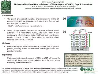
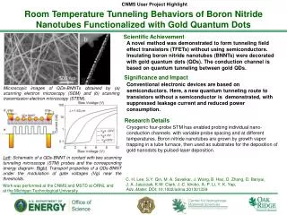
CNMS User Project Highlight Room Temperature Tunneling Behaviors of Boron Nitride Nanotubes Functionalized with Gold Quantum Dots Scientific Achievement (b) (a) A novel method was demonstrated to form tunneling field effect transistors (TFETs) without using semiconductors. Insulating boron nitride nanotubes (BNNTs) were decorated with gold quantum dots (QDs). The conduction channel is based on quantum tunneling between gold QDs. Significance and Impact Conventional electronic devices are based on semiconductors. Here, anew quantum tunneling route to transistors without a semiconductor is demonstrated, with suppressed leakage current and reduced power consumption. Microscopic images of QDs-BNNTs obtained by (a) scanning electron microscopy (SEM) and (b) scanning transmission electron microscopy (STEM). Research Details • Cryogenic four-probe STM has enabled probing individual nano-conduction channels with variable probe spacing and at different temperatures. Boron nitride nanotubes are grown by growth vapor trapping in a tube furnace, then used as substrates for the deposition of gold nanodots by pulsed-laser deposition. Left: Schematic of a QDs-BNNT in contact with two scanning tunneling microscope (STM) probes and the corresponding energy diagram. Right: Transport properties of a QDs-BNNT under the modulation of gate voltages (Vg) near the thresholds. C. H. Lee, S.Y. Qin, M. A. Savaikar, J. Wang, B. Hao, D. Zhang, D. Banyai, J. A. Jaszczak, K.W. Clark, J.-C. Idrobo, A.-P. Li, Y. K. Yap, Adv. Mater. DOI: 10.1002/adma.201301339 Work was performed at the CNMS and MSTD at ORNL and at the Michigan Technological University
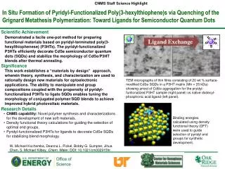
CNMS User Project Highlight Beyond Silicon: Transistors Without Semiconductors Scientific Achievement (b) (a) A novel method has been developed to make a transistor using a nanoscale insulator with nanoscale metals on top. The transistor works at room temeprature via quantum tunneling between metal nanodots, dramatically different from a semiconductor device. Significance and Impact Transistors based on semiconductors can only get so small and they waste a lot of energy in the form of heat. Exploration of a quantum tunneling route to transistors without a semiconductor is important for next generation large scale device integration. Microscopic images of gold nanodots decorated on boron nitride nanotubes obtained by (a) scanning electron microscopy (SEM) and (b) scanning transmission electron microscopy (STEM). Schematic of electrons flash across a series of gold quantum dots on boron nitride nanotubes. The quantum-tunneling device acts like a transistor at room temperature, without using semiconducting materials. Research Details Cryogenic four-probe STM transport spectroscopy enabled probing individual nano-conduction channels with variable probe spacing and at different temperatures. Boron nitride nanotubes are grown by growth vapor trapping in a tube furnace, then used as substrates for the deposition of gold nanodots by pulsed-laser deposition. C. H. Lee, S.Y. Qin, M. A. Savaikar, J. Wang, B. Hao, D. Zhang, D. Banyai, J. A. Jaszczak, K.W. Clark, J.-C. Idrobo, A.-P. Li, Y. K. Yap, Adv. Mater. DOI: 10.1002/adma.201301339 Work was performed at the CNMS and MSTD at ORNL and at the Michigan Technological University