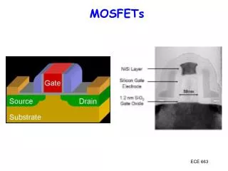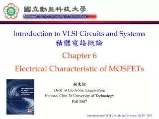
Chapter 6 Electrical Characteristic of MOSFETs
490 likes | 1.6k Vues
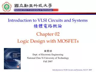
Chapter 6 Electrical Characteristic of MOSFETs. Introduction to VLSI Circuits and Systems 積體電路概論. 賴秉樑 Dept. of Electronic Engineering National Chin-Yi University of Technology Fall 2007. Outline. MOS Physics nFET Current-Voltage Equations The FET RC Model pFET Characteristic

Chapter 6 Electrical Characteristic of MOSFETs
E N D
Presentation Transcript
Chapter 6Electrical Characteristic of MOSFETs Introduction to VLSI Circuits and Systems積體電路概論 賴秉樑 Dept. of Electronic Engineering National Chin-Yi University of Technology Fall 2007
Outline • MOS Physics • nFET Current-Voltage Equations • The FET RC Model • pFET Characteristic • Modeling of Small MOSFETs
MOS Physics • MOSFETs conduct electrical current by using an applied voltage to move charge from the source to drain of the device • Occur only if a conduction path, or channel, has been created • The drain current IDn is controlled by voltages applied to the device (6.1) IDn = IDn(VGSn, VDSn) Figure 6.1 nFET current and voltages
Field-effect • Simple MOS structure • Silicon dioxide (SiO2) acts as an insulator between the gate and substrate • Cox determines the amount of electrical coupling that exists between the gate electrode and the p-type silicon region • What is Field-effect ? • The electric field induces charge in the semiconductor and allows us to control the current flow through the FET by varying the gate voltage VG (C/ cm2) (6.2) Where, tox is the thickness of the oxide in cm Figure 6.2 Structure of the MOS system Figure 6.3 Surface charge density Qs (6.3)
Where, Vox is the voltage drop across the oxide layer and is the surface potential that represents the voltage at the top of the silicon Threshold Voltage • At the circuit level, Vth is obtained by KVL • The oxide voltage Vox is the difference (VG - ) and is the result of a decreasing electric potential inside the oxide (6.4) Figure 6.4 Voltages in the MOS system
Electric Fields of MOS (1/2) • Lorentz law: an electric field exerts a force on a charged particle • A depleted MOS structure cannot support the flow of electrical current (6.5) (positively charged holes) (6.6) (6.7) (negatively charged electrons) Figure 6.5 MOS electric fields (6.8) (bulk charge) Where (the oxide voltage is related to the bulk charge) (6.9) Figure 6.6 Bulk (depletion) charge in the MOS system
Electric Fields of MOS (2/2) • For VG < VTn, the charge is immobile bulk charge and QS = QB • For VG > VTn, the charge is mode up of two distinct components such that • If VG = VTn, then Qe = 0 • If VG > VTn, then (6.10) Where Qe: electron charge layer that electrons are mobile and can move in a lateral direction (parallel to the surface, also called a channel region) (6.11) Figure 6.7 Formation of the electron charge layer
Outline • MOS Physics • nFET Current-Voltage Equations • The FET RC Model • pFET Characteristic • Modeling of Small MOSFETs
nFET • The dimensionless quantity (W/L) is the aspect ratio that is used to specify the relative size of a transistor with respect to others • The MOS structure allows one to control the creation of the electron charge layer Qe under the gate oxide by using the gate-source voltage VGSn (a) Side view (b) Top view (6.19) Figure 6.8 Details of the nFET structure (a) Symbol (b) Structure Figure 6.9 Current and voltages for an nFET
Channel Formation for nFET • Cutoff mode as Figure 6.10 (a) • If VGSn < VTn, then Qe = 0 and IDn = 0 • Like an open switch • Active mode as Figure 6.10 (b) • If VGSn > VTn, then Qe ≠ 0 and IDn = F(VGSn, VDSn) • Like an closed switch (a) Cutoff (b) Active bias Figure 6.10 Controlling the channel in an nFET (a) Cutoff (b) Active Figure 6.11 Channel formation in an nFET
nMOS I–V Characteristics (1/2) • Three region for nMOS • According Figure 6.12 (Model I, VDSn = VDD) (6.20) (saturation current) (βn: device transconductance parameter) (6.21) (A/V2) (k’n: process transconductance parameter) (6.22) (6.23) Figure 6.12 I-V characteristics as a function of VGSn (6.24)
nMOS I – V Characteristics (2/2) • According Figure 6.13 (Model II, VGSn > VTn) (active region current) (6.29) (6.30) (6.31) Figure 6.13 I - V characteristics as a function of VDSn (saturation voltage) (6.32) (6.33) (saturation current) (6.34) Where λ (V-1) is channel length modulation parameter Figure 6.14 nFET family of curves (6.35)
Body-bias Effect • Body-bias effects: occur when a voltage VSBn exists between the source and bulk terminals (6.45) Where γ is the body-bias coefficient with units of V1/2, and is the bulk Fermi potential term1 (6.46) (zero body-bias threshold voltage) Figure 6.15 Bulk electrode and body-bias voltage (6.47) Where q = 1.6 × 10⁻¹⁹ C, εSi = 11.8ε0 is the permittivity of silicon, and Na si the acceptor doping in the p-type substrate
Outline • MOS Physics • nFET Current-Voltage Equations • The FET RC Model • pFET Characteristic • Modeling of Small MOSFETs
Non-linear and Linear • The difference between analysis and design • Since non-linear I-V characteristics issue • Analysis deals with studying a new network from the design, and designers are true problem solvers • Two approaches to dealing with the problem of messy transistor equations • Let circuit specialists deal with the issues introduced by the non-linear devices • Create a simplifies linear model since VLSI design is based on logic and digital architectures (a) nFET symbol (b) Linear model for nFET Figure 6.19 RC model of an nFET
Drain-Source FET Resistance • In practical, FET are inherently non-linear (drain-source resistance) (6.64) (6.65) (at a point in Figure 6.20) (6.66) (6.67) (at b point in Figure 6.20) (6.68) (at c point in Figure 6.20) (6.69) (6.70) Figure 6.20 Determining the nFET resistance (6.71) (6.72)
FET Capacitances • The maximum switching speed of a CMOS circuit is determined by the capacitances • When we have C = C(V), the capacitance is said to be non-linear (6.76) (a) Circuit perspective (b) Physical origin (6.77) Figure 6.21 Gate capacitance in a FET (ideal model) (6.78) Figure 6.22 Gate-source and gate-drain capacitance
Junction Capacitance (1/2) • Semiconductor physics reveals that a pn junction automatically exhibits capacitance due to the opposite polarity charges involved is called junction or depletion capacitance • Such that the total capacitance is (CSB and CDB) • Two complications in applying this formula to the nFET • First, this capacitance also varies with the voltage (C = C(V)) • Second in next slide (6.82) Figure 6.23 Junction capacitance in MOSFET Where Apn is the area of the junction in units of cm2, and Cj is determined by the process, and varies with doping levels (6.83) Figure 6.24 Junction capacitance variation with reverse voltage (built-in potential) (6.84)
Junction Capacitance (2/2) • Second, we need to consider in calculating the pn junction capacitance is the geometry of the pn junctions (6.85) (1. bottom section) (6.86) (6.87) (2. sidewall) (a) Top view (6.88) (sidewall perimeter) (6.89) (6.90) (sidewall capacitance per unit perimeter) (6.91) (including the overlap section) (6.92) (1 + 2) (b) Geometry (non-linear model) Figure 6.25 Calculation of the FET junction capacitance (6.93)
Construction of the Model • Parasitic resistance and capacitance of MOS • It is important to note that the resistance Rn is inversely proportional to the aspect ratio (W/L)n, while the capacitances increase with the channel width W (6.94) Figure 6.26 Physical visualization of FET capacitances (a) nFET (b) Linear model for nFET Figure 6.25 Calculation of the FET junction capacitance
Outline • MOS Physics • nFET Current-Voltage Equations • The FET RC Model • pFET Characteristic • Modeling of Small MOSFETs • Reference for Further Reading • Problems
pFET Characteristic (1/4) • nFET translates to pFET • Change all n-type regions to p-type regions • Change all p-type regions to n-type regions • Note, both the direction of the electric fields and the polarities of the charges will be opposite according equation (6.101) • n-well is tied to the positive power supply Figure 6.29 Transforming an nFET to a pFET (6.101) (a) Side view (b) Top view Figure 6.30 Structural detail of a pFET
pFET Characteristic (2/4) • VSGp determines whether the gate is sufficiently negative with respect to the source to create a layer of holes under the gate oxide and thus establish a positive hole charge density of Qh C/cm2 (a) Symbol (6.102) (6.103) (6.104) (b) Structure Figure 6.31 Current and voltages in a pFET
pFET Characteristic (3/4) (6.105) (6.106) (a) Cutoff (b) Active bias (6.107) Figure 6.32 Conduction modes of a pFET (6.108) (6.109) Figure 6.33 Gate-controlled pFET current-voltage characteristics
pFET Characteristic (4/4) (6.110) (6.111) (6.112) Figure 6.34 pFET I – V family of curves
Outline • MOS Physics • nFET Current-Voltage Equations • The FET RC Model • pFET Characteristic • Modeling of Small MOSFETs
Scaling Theory (1/2) (6.123) (6.118) (6.119) (6.124) (6.120) (6.125) (6.126) (6.121) (6.122) (6.127)
Scaling Theory (2/2) (6.128) (6.129) (6.130) (6.131) (6.132) (6.133)