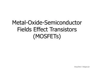
MOSFETs
MOSFETs. A little bit of history. V SG. V SD. More electrons. Operation of a transistor. V SG > 0 n type operation. Gate. Insulator. Source. Drain. Channel. Substrate. Positive gate bias attracts electrons into channel Channel now becomes more conductive . V SG. V SD.

MOSFETs
E N D
Presentation Transcript
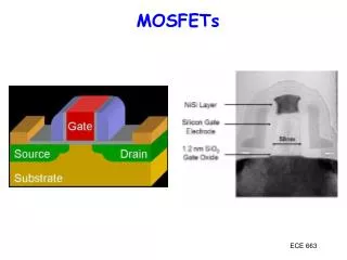
MOSFETs ECE 663
A little bit of history.. ECE 663
VSG VSD More electrons Operation of a transistor VSG > 0 n type operation Gate Insulator Source Drain Channel Substrate Positive gate bias attracts electrons into channel Channel now becomes more conductive
VSG VSD Operation of a transistor Gate Insulator Source Drain Channel Substrate Transistor turns on at high gate voltage Transistor current saturates at high drain bias
VSG VSD Start with a MOS capacitor Gate Insulator Source Drain Channel Substrate
Questions • W What is the MOS capacitance? QS(yS) What are the local conditions during inversion? yS,cr How does the potential vary with position? y(x) How much inversion charge is generated at the surface? Qinv(x,yS) Add in the oxide: how does the voltage divide? yS(VG), yox(VG) How much gate voltage do you need to invert the channel? VTH How much inversion charge is generated by the gate? Qinv(VG) What’s the overall C-V of the MOSFET? QS(VG)
Ideal MIS Diode n-type, Vappl=0 Assume Flat-band at equilibrium qfS EC EF Ei EV ECE 663
Ideal MIS Diode n-type, Vappl=0 ECE 663
Ideal MIS Diode p-type, Vappl=0 ECE 663
Ideal MIS Diode p-type, Vappl=0 ECE 663
Accumulation Pulling in majority carriers at surface ECE 663
But this increases the barrier for current flow !! n+ p n+ ECE 663
Depletion ECE 663
Inversion yB Need CB to dip below EF. Once below by yB, minority carrier density trumps the intrinsic density. Once below by 2yB, it trumps the major carrier density (doping) ! ECE 663
Sometimes mathscan help… ECE 663
P-type semiconductor Vappl0 Convention for p-type: y positive if bands bend down ECE 663
Ideal MIS diode – p-type CB moves towards EF if y > 0 n increases VB moves away from EF if y > 0 p decreases ECE 663
Ideal MIS diode – p-type At the semiconductor surface, = s ECE 663
Surface carrier concentration • s < 0 - accumulation of holes • s =0 - flat band • B>s >0 – depletion of holes • s =B - intrinsic concentration ns=ps=ni • s > B – Inversion (more electrons than holes) EC EF ECE 663
Want to find , E-field, Capacitance • Solve Poisson’s equation to get E field, potential based on charge density distribution(one dimension) E E E ECE 663
Away from the surface, = 0 • and ECE 663
Solve Poisson’s equation: E = -dy/dx d2y/dx2 = -dE/dx = (dE/dy).(-dy/dx) = EdE/dy EdE/dy ECE 663
Solve Poisson’s equation: • Do the integral: • LHS: • RHS: • Get expression for E field (d/dx): ECE 663
Define: Debye Length Then: E > 0 E < 0 y > 0 y < 0 + for > 0 and – for < 0 ECE 663
Accumulation to depletion to strong Inversion • For negative , first term in F dominates – exponential • For small positive , second term in F dominates - • As gets larger, second exponential gets big yB = (kT/q)ln(NA/ni) = (1/b)ln(pp0/√pp0np0) (np0/pp0) = e-2byB yS > 2yB ECE 663
Questions • What is the MOS capacitance? QS(yS) • What are the local conditions during inversion? yS,cr • How does the potential vary with position? y(x) • How much inversion charge is generated at the surface? Qinv(x,yS) • Add in the oxide: how does the voltage divide? yS(VG), yox(VG) • How much gate voltage do you need to invert the channel? VTH • How much inversion charge is generated by the gate? Qinv(VG) • What’s the overall C-V of the MOSFET? QS(VG)
Charges, fields, and potentials • Charge on metal = induced surface charge in semiconductor • No charge/current in insulator (ideal) metal insul semiconductor depletion inversion ECE 663
Charges, fields, and potentials Electrostatic Potential Electric Field ECE 663
Depletion Region Electrostatic Potential Electric Field ECE 663
Depletion Region Electrostatic Potential Electric Field y = ys(1-x/W)2 Wmax = 2es(2yB)/qNA yB= (kT/q)ln(NA/ni) ECE 663
Questions • What is the MOS capacitance? QS(yS) • What are the local conditions during inversion? yS,cr • How does the potential vary with position?y(x) • How much inversion charge is generated at the surface? Qinv(x,yS) • Add in the oxide: how does the voltage divide? yS(VG), yox(VG) • How much gate voltage do you need to invert the channel? VTH • How much inversion charge is generated by the gate? Qinv(VG) • What’s the overall C-V of the MOSFET? QS(VG)
Exact Solution U = by US = byS UB = byB dy/dx = -(2kT/qLD)F(yB,np0/pp0) U dU/F(U) = x/LD US F(U) = [eUB(e-U-1+U)-e-UB (eU-1-U)]1/2
Exact Solution r = qni[eUB(e-U-1) – e-UB(eU-1)] US dU’/F(U’,UB) = x/LD U F(U,UB) = [eUB(e-U-1+U) + e-UB (eU-1-U)]1/2
Exact Solution NA = 1.67 x 10¹⁵ Qinv ~ 1/(x+x0)a x0 ~ LD . factor
Questions • What is the MOS capacitance? QS(yS) • What are the local conditions during inversion? yS,cr • How does the potential vary with position?y(x) • How much inversion charge is generated at the surface? Qinv(x,yS) • Add in the oxide: how does the voltage divide? yS(VG), yox(VG) • How much gate voltage do you need to invert the channel?VTH • How much inversion charge is generated by the gate? Qinv(VG) • What’s the overall C-V of the MOSFET? QS(VG)
Threshold Voltage for Strong Inversion • Total voltage across MOS structure= voltage across dielectric plus s ECE 663
Notice Boundary Condition !! eoxVi/tox = esys/(W/2) Before Inversion After inversion there is a discontinuity in D due to surface Qinv Vox (at threshold) = es(2yB)/(Wmax/2)Ci = ECE 663
VG = Vfb + ys + (kstox/kox) √(2kTNA/e0ks)[bys + eb(ys-2yB)]1/2 Local Potential vs Gate voltage yox ys Initially, all voltage drops across channel (blue curve). Above threshold, channel potential stays pinned to 2yB, varying only logarithmically, so that most of the gate voltage drops across the oxide (red curve).
Look at Effective charge width ~Wdm/2 ~tinv Initially, a fast increasing channel potential drops across increasing depletion width Eventually, a constant potential drops across a decreasing inversion layer width, so field keeps increasing and thus matches increasing field in oxide
Questions • What is the MOS capacitance? QS(yS) • What are the local conditions during inversion? yS,cr • How does the potential vary with position?y(x) • How much inversion charge is generated at the surface? Qinv(x,yS) • Add in the oxide: how does the voltage divide? yS(VG), yox(VG) • How much gate voltage do you need to invert the channel? VTH • How much inversion charge is generated by the gate? Qinv(VG) • What’s the overall C-V of the MOSFET? QS(VG)
Charge vs Local Potential Qs≈√(2e0kskTNA)[bys + eb(ys-2yB)]1/2 Beyond threshold, all charge goes to inversion layer
How do we get the curvatures? NEW Add other terms and keep Leading term EXACT
Inversion Charge vs Gate voltage Q ~ eb(ys-2yB), ys- 2yB ~ log(VG-VT) Exponent of a logarithm gives a linear variation of Qinv with VG Qinv = -Cox(VG-VT) Why Cox?
Questions • What is the MOS capacitance? QS(yS) • What are the local conditions during inversion? yS,cr • How does the potential vary with position?y(x) • How much inversion charge is generated at the surface? Qinv(x,yS) • Add in the oxide: how does the voltage divide? yS(VG), yox(VG) • How much gate voltage do you need to invert the channel? VTH • How much inversion charge is generated by the gate? Qinv(VG) • What’s the overall C-V of the MOSFET?QS(VG)
Capacitance For s=0 (Flat Band): Expand exponentials….. ECE 663
Capacitance of whole structure • Two capacitors in series: Ci - insulator CD - Depletion OR ECE 663
Capacitance vs Voltage ECE 663