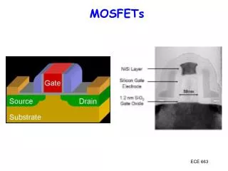
Introduction to MOSFETs
Introduction to MOSFETs. Figure 4.1 Physical structure of the enhancement-type NMOS transistor: (a) perspective view; (b) cross-section. Typically L = 0.1 to 3 m m, W = 0.2 to 100 m m, and the thickness of the oxide layer ( t ox ) is in the range of 2 to 50 nm.

Introduction to MOSFETs
E N D
Presentation Transcript
Figure 4.1 Physical structure of the enhancement-type NMOS transistor: (a) perspective view; (b) cross-section. Typically L = 0.1 to 3 mm, W = 0.2 to 100 mm, and the thickness of the oxide layer (tox) is in the range of 2 to 50 nm. Figure 4.10 (a) Circuit symbol for the n-channel enhancement-type MOSFET. (b) Modified circuit symbol with an arrowhead on the source terminal to distinguish it from the drain and to indicate device polarity (i.e., n channel). (c) Simplified circuit symbol to be used when the source is connected to the body or when the effect of the body on device operation is unimportant.
Figure 4.2 The enhancement-type NMOS transistor with a positive voltage applied to the gate. An n channel is induced at the top of the substrate beneath the gate. Figure 4.4 The iD–vDS characteristics of the MOSFET in Fig. 4.3 when the voltage applied between drain and source, vDS, is kept small. The device operates as a linear resistor whose value is controlled by vGS.
Figure 4.5 Operation of the enhancement NMOS transistor as vDSis increased. The induced channel acquires a tapered shape, and its resistance increases as vDS is increased. Here, vGS is kept constant at a value > Vt. Figure 4.7 Increasing vDS causes the channel to acquire a tapered shape. Eventually, as vDS reaches vGS– Vt’ the channel is pinched off at the drain end. Increasing vDS above vGS– Vthas little effect (theoretically, no effect) on the channel’s shape.
Figure 4.6 The drain current iD versus the drain-to-source voltage vDS for an enhancement-type NMOS transistor operated with vGS> Vt. Figure 4.11 (a) An n-channel enhancement-type MOSFET with vGS and vDS applied and with the normal directions of current flow indicated. (b) The iD–vDS characteristics for a device with k’n(W/L) = 1.0 mA/V2.
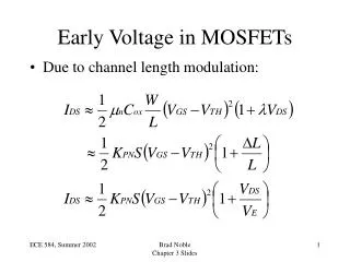
Figure 4.12 The iD–vGS characteristic for an enhancement-type NMOS transistor in saturation (Vt = 1 V, k’nW/L = 1.0 mA/V2). Figure 4.15 Increasing vDS beyond vDSsatcauses the channel pinch-off point to move slightly away from the drain, thus reducing the effective channel length (by DL). Figure 4.16 Effect of vDS on iD in the saturation region. The MOSFET parameter VA depends on the process technology and, for a given process, is proportional to the channel length L.
Figure 4.26(a) Basic structure of the common-source amplifier. (b) Graphical construction to determine the transfer characteristic of the amplifier in (a). Figure 4.26(Continued)(c) Transfer characteristic showing operation as an amplifier biased at point Q.
Figure 4.9 Cross-section of a CMOS integrated circuit. Note that the PMOS transistor is formed in a separate n-type region, known as an n well. Another arrangement is also possible in which an n-type body is used and the n device is formed in a p well. Not shown are the connections made to the p-type body and to the n well; the latter functions as the body terminal for the p-channel device. Figure 4.18(a) Circuit symbol for the p-channel enhancement-type MOSFET. (b) Modified symbol with an arrowhead on the source lead. (c) Simplified circuit symbol for the case where the source is connected to the body. (d) The MOSFET with voltages applied and the directions of current flow indicated. Note that vGS and vDS are negative and iD flows out of the drain terminal. Body effect…