4446 Design of Microprocessor-Based Systems
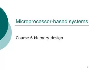
4446 Design of Microprocessor-Based Systems. I/O System Design. Dr. Esam Al_Qaralleh CE Department Princess Sumaya University for Technology. Data bus. AL. AX. I/O. I/O. I/O. 8088. Address bus A[15:0]. Introduction (cont’d). 65,536 possible I/O ports.

4446 Design of Microprocessor-Based Systems
E N D
Presentation Transcript
4446 Design of Microprocessor-Based Systems I/O System Design Dr. Esam Al_Qaralleh CE Department Princess Sumaya University for Technology
Data bus AL AX I/O I/O I/O 8088 Address bus A[15:0] Introduction (cont’d) • 65,536 possible I/O ports • Data transfer between ports and the processor is over data bus • 8088 uses address bus A[15:0] to locate an I/O port • AL (or AX) is the processor register that takes input data (or provide output data)
Introduction • I/O devices serve two main purposes • To communicate with outside world • To store data • I/O controller acts as an interface between the systems bus and I/O device • Relieves the processor of low-level details • Takes care of electrical interface • I/O controllers have three types of registers • Data • Command • Status
Introduction (cont’d) • To communicate with an I/O device, we need • Access to various registers (data, status,…) • This access depends on I/O mapping • Two basic ways • Memory-mapped I/O • Isolated I/O • A protocol to communicate (to send data, …) • Three types • Programmed I/O • Direct memory access (DMA) • Interrupt-driven I/O
Accessing I/O Devices • I/O address mapping • Memory-mapped I/O • Reading and writing are similar to memory read/write • Uses same memory read and write signals • Most processors use this I/O mapping • Isolated I/O • Separate I/O address space • Separate I/O read and write signals are needed • Pentium supports isolated I/O • 64 KB address space • Can be any combination of 8-, 16- and 32-bit I/O ports • Also supports memory-mapped I/O FFFFF FFFFF Memory addressing space I/O FFFF I/O addressing space Memory addressing space 00000 00000 0000 Direct I/O Memory-mapped I/O
Accessing I/O Devices (cont’d) • Accessing I/O ports in 80x86 • Register I/O instructions in accumulator, port8 ; direct format • Useful to access first 256 ports in accumulator,DX ; indirect format • DX gives the port address • Block I/O instructions • ins and outs • Both take no operands---as in string instructions • ins: port address in DX, memory address in ES:(E)DI • outs: port address in DX, memory address in ES:(E)SI • We can use rep prefix for block transfer of data
8088 Port Addressing Space • Addressing Space • Accessing directly by instructions IN AL, 80H IN AX, 6H OUT 3CH, AL OUT 0A0H, AX FFFF • Accessing through DX Accessed through DX IN AL, DX IN AX, DX OUT DX, AL OUT DX, AX 00FF Accessed directly by instructions 00F8 0000
Input Port Implementation Data Bus Gating device Input 8088 Address bus Decoder Other control signals • The outputs of the gating device are high impedance when the processor is not accessing the input port • When the processor is accessing the input port, the gating device transfers input data to CPU data bus • The decoding circuit controls when the gating device has high impedance output and when it transfers input data to data bus
A7 Tri-state buffer A6 Data bus Input data A5 A4 A3 CE A2 A1 A0 RD IO/M Input Port Implementation • Circuit Implementation • Assume that the address of the input port is 9CH
A7 A6 Data bus Latch Output data A5 A4 A3 CLK A2 A1 A0 WR IO/M Output Port Implementation • Circuit Implementation • Assume that the address of the output port is 9CH
R A=B B3 A7 A3 B2 A2 A6 B1 A5 A1 B0 A4 A0 A=B A=B B3 A3 A3 B2 A2 A2 B1 A1 A1 B0 A0 A0 A=B RD or WR IO/M A Reconfigurable Port Decoder 1 Vcc
An Example I/O Device • Keyboard • Keyboard controller scans and reports • Key depressions and releases • Supplies key identity as a scan code • Scan code is like a sequence number of the key • Key’s scan code depends on its position on the keyboard • No relation to the ASCII value of the key • Interfaced through an 8-bit parallel I/O port • Originally supported by 8255 programmable peripheral interface chip (PPI)
An Example I/O Device (cont’d) • 8255 PPI has three 8-bit registers • Port A (PA) • Port B (PB) • Port C (PC) • These ports are mapped as follows 8255 register Port address PA (input port) 60H PB (output port) 61H PC (input port) 62H Command register 63H
An Example I/O Device (cont’d) Mapping of 8255 I/O ports
An Example I/O Device (cont’d) • Mapping I/O ports is similar to mapping memory • Partial mapping • Full mapping • Keyboard scan code and status can be read from port 60H • 7-bit scan code is available from • PA0 – PA6 • Key status is available from PA7 • PA7 = 0 – key depressed • PA0 = 1 – key released
I/O Data Transfer • Data transfer involves two phases • A data transfer phase • It can be done either by • Programmed I/O • DMA • An end-notification phase • Programmed I/O • Interrupt • Three basic techniques • Programmed I/O • DMA • Interrupt-driven I/O
I/O Data Transfer (cont’d) • Programmed I/O • Done by busy-waiting • This process is called polling • Example • Reading a key from the keyboard involves • Waiting for PA7 bit to go low • Indicates that a key is pressed • Reading the key scan code • Translating it to the ASCII value • Waiting until the key is released
Data bus D[7:0] PA[7:0] A0 8088 PB[7:0] A1 RD Control port WR PC[7:0] RESET A7 CS A6 A5 A4 A3 A2 Port IO/M A1 A0 • 0 0 • 0 1 • 0 • 1 1 PA PB PC Control 8255 Programmable Peripheral Interface
Programming 8255 • 8255 has three operation modes: mode 0, mode 1, and mode 2
PA[7:0] PA[7:0] PC4 STBA PC7 OBFA PC5 IBFA PC6 ACKA PC3 INTRA PC3 INTRA 8255 8255 PB[7:0] PB[7:0] PC2 STBB PC2 OBFB PC1 IBFB PC1 ACKB PC0 INTRB PC0 INTRB PC6, 7 PC4, 5 Programming 8255 • Mode 0: • Ports A, B, and C can be individually programmed as input or output ports • Port C is divided into two 4-bit ports which are independent from each other • Mode 1: • Ports A and B are programmed as input or output ports • Port C is used for handshaking
PA[7:0] PC7 OBFA PC6 ACKA PC4 STBA PC5 IBFA 8255 PC3 INTRA PC0 In Out In Out In Out STBB OBFB IBFB ACKB INTRB INTRB PC0 PC0 PB[7:0] Mode 1 Mode 0 Programming 8255 • Mode 2: • Port A is programmed to be bi-directional • Port C is for handshaking • Port B can be either input or output in mode 0 or mode 1 • Can you design a decoder for an 8255 chip such that its base address is 40H? • Write the instructions that set 8255 into mode 0, port A as input, port B as output, PC0-PC3 as input, PC4-PC7 as output ?
Timing diagram is a combination of the Mode 1 Strobed Input and Mode 1 Strobed Output Timing diagrams.
BIT5 EQU 20H PORTC EQU 22H PORTA EQU 20H READ PROC NEAR Read: IN AL, PORTC ; read portc TEST AL, BIT5 ;test IBF JZ Read ;if IBF=0 IN AL, PORTA ;Read Data READ ENDP Example: Mode 1 Input keyboard 8255 PA0 PA7 STB PC4 DAV
Example: Mode 1 output Printer 8255 PB0 PB7 Data Strobe : to tell the printer to latch the incoming data. Generated Externally ACK PC2 ACK PC4 DS
BIT1 EQU 2 PORTC EQU 62H PORTB EQU 61H CMD EQU 63H PRINT PROC NEAR ; check printer ready? IN AL, PORTC ;get OBF TEST AL, BIT1 ;test OBF JZ PRINT ;if OBF=0 buffer is full ;send character to printer MOV AL, AH ;get data OUT PORTB, AL ;print data ; send data strobe to printer MOV AL, 8 ;clear DS OUT CMD, AL MOV AL, 9 ;clear DS OUT CMD, AL ;rising the data at the positive edge of DS RET PRINT ENDP Example: Mode 1 output
De-bouncing Circuitry Two asynchronous flip-flop solutions are given below • The basic idea is that these flip-flops store the values even if the D/D nodes both float
External Interface • Two ways of interfacing I/O devices • Serial • Cheaper • Slower • Parallel • Faster • Data skew Limited to small distances
External Interface (cont’d) Two basic modes of data transmission
External Interface (cont’d) • Serial transmission • Asynchronous • Each byte is encoded for transmission • Start and stop bits • No need for sender and receiver synchronization • Synchronous • Sender and receiver must synchronize • Done in hardware using phase locked loops (PLLs) • Block of data can be sent • More efficient • Less overhead than asynchronous transmission • Expensive
External Interface (cont’d) Asynchronous transmission
External Interface (cont’d) • EIA-232 serial interface • Low-speed serial transmission • Adopted by Electronics Industry Association (EIA) • Popularly known by its predecessor RS-232 • It uses a 9-pin connector DB-9 • Uses 8 signals • Typically used to connect a modem to a computer
External Interface (cont’d) • Transmission protocol uses three phases • Connection setup • Computer A asserts DTE (Data Terminal Equipment) Ready • Transmits phone# via Transmit Data line (pin 2) • Modem B alerts its computer via Ring Indicator (pin 9) • Computer B asserts DTE Ready (pin 4) • Modem B generates carrier and turns its DCE (Data Communication Equipment) Ready • Modem A detects the carrier signal from modem B • Modem A alters its computer via Carrier Detect (pin 1) • Turns its DCE Ready • Data transmission • Done by handshaking using • request-to-send (RTS) and clear-to-send (CTS) signals • Connection termination • Done by deactivating RTS
External Interface (cont’d) • Parallel printer interface • A simple parallel interface • Uses 25-pin DB-25 • 8 data signals • Latched by strobe (pin 1) • Data transfer uses simple handshaking • Uses acknowledge (CK) signal • After each byte, computer waits for ACK • 5 lines for printer status • Busy, out-of-paper, online/offline, autofeed, and fault • Can be initialized with INIT • Clears the printer buffer and resets the printer
Start bit B0 B1 B2 B3 B4 B5 B6 Stop bits Parity Serial Data Transfer • Asynchronous v.s. Synchronous • Asynchronous transfer does not require clock signal. However, it transfers extra bits (start bits and stop bits) during data communication • Synchronous transfer does not transfer extra bits. However, it requires clock signal Frame data Asynchronous Data transfer clk Synchronous Data transfer data B0 B1 B2 B3 B4 B5 Baud (Baud is # of bits transmitted/sec, including start, stop, data and parity).
8251 RS232 D[7:0] TxD RD RD RxD WR WR A0 C/D TxC CLK CLK RxC A7 A6 A5 A4 A3 A2 A1 IO/M 8251 USART Interface