Download
1 / 11
140 likes | 365 Vues
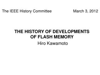
THE HISTORY OF DEVELOPMENTS OF FLASH MEMORY Hiro Kawamoto. The IEEE History Committee March 3, 2012. Structures of Non-Volatile Memory. 1967-1971. 1967 USE of FIELD-EFFECT TRANSISTOR FLOATING GATE for CHARGE STORAGE WRITE by TUNNELING ERASE by TUNNELING

E N D
THE HISTORY OF DEVELOPMENTS OF FLASH MEMORYHiro Kawamoto The IEEE History Committee March 3, 2012
1967-1971 • 1967 • USE of FIELD-EFFECT TRANSISTOR • FLOATING GATE for CHARGE STORAGE • WRITE by TUNNELING • ERASE by TUNNELING • D. Kahng and S. M. Sze, “A floating gate and its application to memory devices,” Bell Syst. Tech. J., (46) p.1288 (1967) [Ref: Flash Memory Kahng and Sze paper] • What was new: More recent innovations are directed toward obtaining controlled charging sites in the gate insulation itself to allow charge-storage. The first application of this concept was realized by the use of a floating gate, wherein charge communication with the underlying Si bulk for both electrical write-in and electrical erase was obtained by a tunneling.” The non-volatile memory fabricated by them was a forerunner of current flash memory, which contained all the key components: a floating gate buried in a field-effect transistor, the Fowler-Nordheim tunneling for both writing and erasing, and a
1970-1971 • 1970 • WRITE by AVALNCHE EFFECT • ERASE by ULTRA-VIOLET RADAITION • COMMERCIAL EPROM PRODUCT • June 19, 1970 applied, May 2, 1972 Patent 3,660,819, Dov Frohman-entchkowsky, “FLOATING GATE TRANSISTOR AND METHOD FOR CHARGING AND DISCHARGING SAME” [Flash Memory Frohman patent EPROM] • What was new: Frohman of Intel achieved the write-in by an avalanche effect and the erase by applying ultra-violet light. • In 1971, Intel offered the first commercial product named EPROM (Electrically Programmable Read Only Memory). [Re3f: Flash Memory Frohman Intel1702 of 1971 Intel Museum Exhibit] • 1971 • ERASE by AVANNCHE EFFECT • Yasuo Tarui, Yutaka Hayashi, and Kiyoko Nagai of ELECTROTECHNICAL LABORATORY in Tsukuba, Japan, ”Proposal of Electrically Reprogrammable, Nonvolatile Semiconductor Memory” Proc. 3rd Conf. on Solid State Devices, Tokyo, p.155 (1971) [Flash Memory Tarui paper] • What was new: The first attempt to use avalanche effect for erasing, thus do both write-in and erase electrically, not by UV radiation.
1977-1982 • 1977 EEPROM PROTOTYPE • 1982 COMMERCIAL PRODUCT • Filed: Feb. 22, 1977: Sep 26, 1978 US Pat. 4,115,914, Eli Harai “ELECTRICALLY ERASABLE NON-VOLATILE SEMICONDUCTOR MEMORY” [Flash Memory Harari patent] • (Quote from the SCV's Nomination): 1967: Harari (of Hughes) invents the first practical Floating Gate EEPROM, an electrically-erasable floating gate device using a thin gate oxide at a range of 100 Å, and which included the use of Fowler-Nordheim tunneling for both write and erase operations. Importantly, the practicality of this Floating Gate EEPROM resulted from (1) the fact that this thin SiO2 was sufficiently thick (approx. 70-100 Ã…) to indefinitely store a floating gate charge for data storage, and (2) the use of polysilicon floating gates which were widely adopted in EPROM devices. • In 1982 Hughes offered a Hughes3108 commercial EEPROM product. • (Quote from Wikipedia) • In 1988, SanDisk Corporation (NASDAQ: SNDK) was founded by Dr. Eli Harari and Sanjay Mehrotra. It subsequently commercially offered EEPROM. [Flash Memory Harari San Disk 1988 Wikipidia] • What was new: no new development nor event • (Kawamoto’s Comments): • Above statements in the Nomination are substantially incorrect. (1) Harari’s patent was not filed in 1976, it was filed in 1977. (2) Harari did not “invent” the first practical Floating Gate EEPROM, an electrically-erasable floating gate device which included the use of Fowler-Nordheim tunneling for both write and erase operations. Rather, as shown in the the 1967 Section above, this basic structure was “invented” by Kahng and Sze back in 1967. (3) Nothing new about the use of thin silicon dioxide. There were a lot of research going on silicon dioxide in late 1960s and early 1970s; just to mention a few, started fom M.A. Atalla of Bell Lab (1960), E.H.Snow of Fairchild (1965), and even Andy Grove’s 1967 text book “Physics and Technology of Semiconductor Devices;” then the Director of Fairchild Research Lab. The use of silicon dioxide in silicon devices had already been a subject of Nobel Prize (J.S.Kilby). Nothing new about the use of polysilicon for the floating gate. As the Nominator says, it was already widely been used in non-volatile memories in 1970s. (4) Harari ‘s device was not “the first practical” EEPROM; because it did not become a commercial offered product right after his work in 1977. In 1979 Harari left Hughes, and in 1982 remaining engineers offered a Hughes3108 commercial product [Flash Memory Harari Hughes3108].
1978-1980 • 1980 • COMMERCIALLY OFFERED EEPROM • -Dec 15, 1978 applied, May 13, 1980, US Patent 4,230,158, Dov Frohman-Bentchkowsky, Jerry Mar, George Perlegos, William S. Johnson of Intel, "Electrically programmable and erasable MOS floating memory device employing tunneling and method of fabricating same" [Flash Memory Frohman patent EEPROM] • -In 1980 Intel introduces an industry first Electrically Programmable Read Only Memory Intel 2816 [Flash Memory Frohman Intel 2816, Intel Museum Exhibit] • What was new: The first commercially offered EEPROM • Frohman-Bentchkowsky, et al. improved the method of erasing by using the Fowler-Nordheim tunneling effect for injecting holes to the floating gate, thus does not deteriorate the insulator layer while erasing. Though the basic structure had been firstly proposed by Kahng and Sze back in 1967, this was the first commercial product that realized the proposal.
1981-1987 1981 FLASH ERASING Nov 13, 1981 applied, Masuoka of Toshiba, US Patent,531,203 [Flash Memory Matsuoka patent Flash} What was new: The idea of easing in a flash motion was proposed. Masuoka, et al. of Toshiba proposed an erasing in one shot a large number of bits, rather than erasing bit-by-bit. This substantially reduced the silicon area required for memory chip thus significantly contributed to the reduction of price of EEPROM. 1984 NAMING of FLASH MEMORY Their 1984 IEDM paper coined the name “flash memory.” The name was created because the erasure of a large number of bits in one shot reminded them the flash of camera. [Flash Memory Matsuoka paper 1984 IEDM] 1987 COMMERCIALLY OFFERED FLASH MEMORY What was new: In 1987, Toshiba commercially offered the first flash memory product. [Flash Memory Masuoka Press Release Toshiba]
1987-1991 • 1987 • USE of NAND FORMAT • Matsuoka, et al. of Toshiba proposed to use NAND circuit for EEPROM. This further reduced the silicon area required for a memory chip. [Flash Memory Matsuoka paper 1987 IEDM] • 1991 • COMMERCIALLY OFFERED NAND MEMORY • Toshiba offered the first commercial NAND type flash memory product. [Flash Memory Matsuoka NAND Press Release]
Flash Memory World-Wide Shipment IHS iSuppli
NAND flash shipment by company IHS iSuppli
NOR flash shipment by company IHS iSuppli